 ChipApex | Global Electronic Components Supplier
SEARCH
Search Product
Search Post
— IC芯片 | 连接器 | 传感器 | 被动器件 —
Search productSearch post
— IC芯片 | 连接器 | 传感器 | 被动器件 —
Consult the customer manager about the wholesale price.
consultation hotline:86-132-6715-2157
email:[email protected]
Contact the product manager for consultation. One-stop consultation is available.
Do you want a lower wholesale price? Please send us your inquiry and we will reply immediately.
The SI5017-D-GM is a fully integrated clock and data recovery (CDR) IC with an embedded limiting amplifier, designed for OC-48/STM-16 SONET/SDH applications. It supports data rates up to 2.7 Gbps when utilizing Forward Error Correction (FEC). The device utilizes Silicon Laboratories DSPLL technology to eliminate external loop filter components, thereby reducing jitter generation to a typical value of 3.0 mUIrms. Operating from a single 3.3 V supply within the industrial temperature range of –40 °C to 85 °C, it features differential CML inputs and outputs. Key functional blocks include lock detection, loss-of-signal monitoring, and bit-error-rate alarms.
The SI5017-D-GM is identified as a discontinued product by the manufacturer. Verification of availability requires checking authorized distributors for remaining stock or surplus inventory. Designers should confirm end-of-life status and plan for component obsolescence management prior to procurement.
Select this component for high-speed serial communication systems requiring low jitter recovery without external analog loop filters. Ensure the application operates within the 3.135 V to 3.465 V supply range and –40 °C to 85 °C temperature limits. Verify that the input signal meets the minimum differential swing requirements specified in the electrical characteristics table.
This part belongs to the Si5017 series of high-speed CDRs developed using DSPLL technology. It is distinct from programmable oscillators (Si501/2/3/4) or other power management ICs sharing similar numerical prefixes. The 'D' suffix typically denotes specific packaging or temperature grade variations within the Skyworks/Silicon Labs portfolio.
As a discontinued component, direct replacements are not officially listed in the provided documentation. Engineers must evaluate alternative CDRs with compatible pinouts, DSPLL-like architecture, and support for OC-48/STM-16 rates. Cross-referencing with newer generations of SONET/SDH retimers is recommended.
The LOS threshold is set by applying a voltage to the LOS_LVL pin. A voltage between 1.50 V and 2.50 V maps to a threshold range of 0 to 40 mVpp. Applying less than 1 V disables the LOS function.
The Lock-to-Reference (LTR) input forces the PLL to lock to an external reference clock when asserted. This maintains a stable output clock during alarm conditions such as Loss-of-Signal.
Yes, the device can perform clock and data recovery without an external reference. This is configured by tying REFCLK+ to VDD and REFCLK– to GND, though acquisition time may be longer compared to reference-based operation.
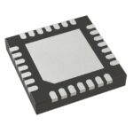 SI5017-D-GM
The activity of extra discounts on wholesale prices is in full swing…
Please fill in your contact information and we will send you the latest wholesale price list.





