ChipApex | Global Electronic Components Supplier
SEARCH
Search Product
Search Post
— IC芯片 | 连接器 | 传感器 | 被动器件 —
Search productSearch post
— IC芯片 | 连接器 | 传感器 | 被动器件 —
Consult the customer manager about the wholesale price.
consultation hotline:86-132-6715-2157
email:[email protected]
Contact the product manager for consultation. One-stop consultation is available.
Do you want a lower wholesale price? Please send us your inquiry and we will reply immediately.
The Si5018-BM is a fully integrated low-power Clock and Data Recovery (CDR) IC designed for high-speed serial communication systems operating at OC-48/STM-16 rates. It utilizes DSPLL™ technology to eliminate external loop filter components, ensuring optimal jitter performance. The device supports data streams up to 2.7 Gbps with Forward Error Correction (FEC). It operates from a single 2.5 V supply over the industrial temperature range of –40 to 85 °C. Key electrical parameters include a typical power dissipation of 270 mW, an output clock rate of 2.4–2.7 GHz, and RMS jitter generation of 3.0 mUI.
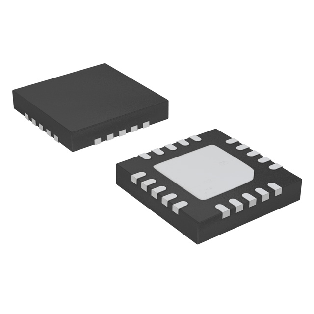
Verify the package type matches the 20-pin Micro Leadframe Package (MLP) with a 4x4 mm footprint. Confirm the temperature grade corresponds to the industrial range (-40 to 85 °C). Ensure the ordering suffix aligns with the specific die revision and designator required for the application.
Select this component for applications requiring low jitter CDR solutions in SONET/SDH environments. The DSPLL™ feature simplifies PCB layout by removing external analog loop filter components. Ensure the system reference clock falls within the specified range of 19.44 MHz to 168.75 MHz for proper PLL centering.
The Si5018-BM is part of the SiPHY™ family of OC-48/STM-16 CDR ICs with FEC. It is manufactured by Silicon Laboratories Inc. The 'BM' suffix denotes the 20-pin MLP package variant suitable for surface mount assembly.
Public confirmed substitute part numbers are not available in the provided documentation. Evaluate compatibility based on pinout, electrical specifications, and package dimensions if considering alternative CDR devices.
Self-calibration is initiated by forcing a high-to-low transition on the PWRDN/CAL pin while a valid reference clock is supplied. The pin must be held high for at least 1 µs before transitioning low.
The REXT pin is used to connect an external 10 kΩ (1%) resistor to GND. This resistor sets the internal bias currents, which significantly reduces power consumption compared to implementations using internal resistors.
The LOL pin is driven high when the recovered clock frequency deviates from the reference clock by more than the specified threshold (e.g., 450-750 ppm). It indicates that the PLL has lost frequency lock with the incoming data stream.
 SI5018-BM
The activity of extra discounts on wholesale prices is in full swing…
Please fill in your contact information and we will send you the latest wholesale price list.