 ChipApex | Global Electronic Components Supplier
SEARCH
Search Product
Search Post
— IC芯片 | 连接器 | 传感器 | 被动器件 —
Search productSearch post
— IC芯片 | 连接器 | 传感器 | 被动器件 —
Consult the customer manager about the wholesale price.
consultation hotline:86-132-6715-2157
email:[email protected]
Contact the product manager for consultation. One-stop consultation is available.
Do you want a lower wholesale price? Please send us your inquiry and we will reply immediately.
The SI52131-A11AGM is a PCIe clock generator providing two differential outputs and one buffered single-ended reference clock. It accepts a 25 MHz crystal or clock input to generate compliant frequencies for PCIe Gen 1, Gen 2, and Gen 3 specifications. The device operates on a 3.3 V supply with a typical dynamic current of 45 mA. Key electrical parameters include a cycle-to-cycle jitter of 50 ps maximum for differential outputs and a long-term accuracy of 100 ppm. It features pin-selectable frequency options (100, 125, 200 MHz) and spread spectrum control within a 24-pin QFN package.
Verify the specific ordering suffix against the manufacturer's official documentation. The 'GM' suffix indicates a 24-pin QFN package in an extended temperature range (-40°C to +85°C). Confirm whether the required variant is the tray-packaged 'GM' version or the tape-and-reel 'GMR' version, as packaging differences exist within the family.
Select this component when a dual-differential clock source with a dedicated 25 MHz reference is required for PCIe applications. Ensure the design utilizes a parallel resonance crystal with appropriate load capacitance (12–15 pF) to achieve specified long-term accuracy. Verify that the 3.3 V power supply meets the ±5% tolerance requirements for stable operation.
This part belongs to the Skyworks Si52131 series of high-performance clock generators. The A11A designation specifies the functional configuration including the 25 MHz reference output and specific frequency/spread capabilities. The device is designed for consumer and embedded applications requiring low power consumption and small footprint solutions.
Publicly confirmed substitute part numbers are not available in the provided documentation. Designers should consult Skyworks technical support or the ClockBuilder Pro tool for validated alternatives if the SI52131-A11AGM is unavailable.
Spread spectrum is enabled by setting the SS0 pin high while keeping the SS1 pin low (SS1=0, SS0=1). This configures the differential outputs to -0.5% down spread at a modulation frequency of approximately 31.5 kHz.
The default state for the SS pins is 00, which corresponds to a 100 MHz differential output frequency with spread spectrum disabled.
Yes, the 25 MHz reference output can be disabled by pulling the OE_REF1 pin high or by setting the corresponding bit in Control Register 0 via the I2C interface.
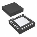 SI52131-A11AGM
The activity of extra discounts on wholesale prices is in full swing…
Please fill in your contact information and we will send you the latest wholesale price list.





