 ChipApex | Global Electronic Components Supplier
SEARCH
Search Product
Search Post
— IC芯片 | 连接器 | 传感器 | 被动器件 —
Search productSearch post
— IC芯片 | 连接器 | 传感器 | 被动器件 —
Consult the customer manager about the wholesale price.
consultation hotline:86-132-6715-2157
email:[email protected]
Contact the product manager for consultation. One-stop consultation is available.
Do you want a lower wholesale price? Please send us your inquiry and we will reply immediately.
The Si52202-A02AGMR is a two-output PCIe clock generator from Skyworks Solutions, designed for 1.5 V to 1.8 V applications supporting PCIe Gen 1 through Gen 7 and SRIS architectures. It provides two 100 MHz differential LP-HCSL outputs compliant with common clock and separate reference specifications. The device features individual hardware control pins and I²C interfaces for output enable, spread spectrum selection (0.25% or 0.5%), and frequency configuration. It includes internal impedance matching options of 100 Ω or 85 Ω to eliminate external resistors. The component operates within an extended temperature range of –40 °C to 85 °C and utilizes a compact 20-pin QFN package.
Verify the specific internal termination resistance required by the design, as the A02 suffix typically denotes 85 Ω matching. Confirm the package variant matches the 20-pin QFN footprint. Ensure the input clock source aligns with the 25 MHz crystal or clock input specification. Check for RoHS compliance documentation if environmental regulations apply to the target assembly.
Select this model when only two differential PCIe clock outputs are needed, optimizing board space compared to higher-output family members. Verify that the fixed 100 MHz output frequency meets system requirements, as other frequencies require factory consultation. Ensure the design accommodates the separate VDD and VDD_IO power supply rails ranging from 1.5 V to 1.8 V and 1.05 V to 1.8 V respectively.
The Si52202 is part of the Si522xx family, which also includes the Si52212 (12 outputs), Si52208 (8 outputs), and Si52204 (4 outputs). All devices share similar architectural features, including LP-HCSL drivers and I²C configurability, but differ in pin count and output capacity. The Si52202 specifically targets applications requiring minimal footprint with dual-channel PCIe timing.
Direct replacements within the same family include Si52202-A01AGMR, which differs primarily in internal termination resistance (100 Ω vs. 85 Ω). Other family members like Si52204 or Si52208 provide additional outputs but require different footprints and pin configurations.
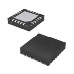 SI52202-A02AGMR
The activity of extra discounts on wholesale prices is in full swing…
Please fill in your contact information and we will send you the latest wholesale price list.





