 ChipApex | Global Electronic Components Supplier
SEARCH
Search Product
Search Post
— IC芯片 | 连接器 | 传感器 | 被动器件 —
Search productSearch post
— IC芯片 | 连接器 | 传感器 | 被动器件 —
Consult the customer manager about the wholesale price.
consultation hotline:86-132-6715-2157
email:[email protected]
Contact the product manager for consultation. One-stop consultation is available.
Do you want a lower wholesale price? Please send us your inquiry and we will reply immediately.
The Si52208-A01AGMR is a low-power clock generator from the Si522xx family, designed for PCIe Gen 1 through Gen 7 and SRIS applications. It provides eight 100 MHz differential LP-HCSL outputs and one 25 MHz LVCMOS reference clock. The device operates on a 1.5 V to 1.8 V supply with separate VDD and VDD_IO rails. Key electrical parameters include a maximum RMS jitter of 0.085 ps and an operating temperature range of –40 °C to +85 °C. It features internal 100 Ω or 85 Ω line matching and supports triangular spread spectrum modulation for EMI reduction.
Verify the specific ordering suffix against the manufacturer's current documentation to confirm package type and tape/reel specifications. Confirm RoHS compliance status via the Certificate of Conformance. Ensure the design accounts for the required humidity sensitivity handling procedures during assembly.
Select the Si52208 when eight differential clock outputs are required for high-port-count designs. Compare power consumption metrics against the Si52212 (12-output) and Si52204 (4-output) variants to optimize board space and energy efficiency. Verify that the 1.5 V to 1.8 V supply voltage aligns with the target system architecture.
This component belongs to the Si522xx family, which includes the Si52212, Si52204, and Si52202 models. These devices share common architectural features such as PLL control, memory, and I2C interfaces but differ in output count and package size. The Si52208 specifically utilizes a 48-pin QFN package to balance port density with footprint constraints.
Direct functional replacements within the same family include the Si52212 (higher output count) and Si52204 (lower output count). Cross-family substitution requires verification of pin compatibility and electrical parameter alignment.
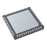 SI52208-A01AGMR
The activity of extra discounts on wholesale prices is in full swing…
Please fill in your contact information and we will send you the latest wholesale price list.






