ChipApex | Global Electronic Components Supplier
SEARCH
Search Product
Search Post
— IC芯片 | 连接器 | 传感器 | 被动器件 —
Search productSearch post
— IC芯片 | 连接器 | 传感器 | 被动器件 —
Consult the customer manager about the wholesale price.
consultation hotline:86-132-6715-2157
email:[email protected]
Contact the product manager for consultation. One-stop consultation is available.
Do you want a lower wholesale price? Please send us your inquiry and we will reply immediately.
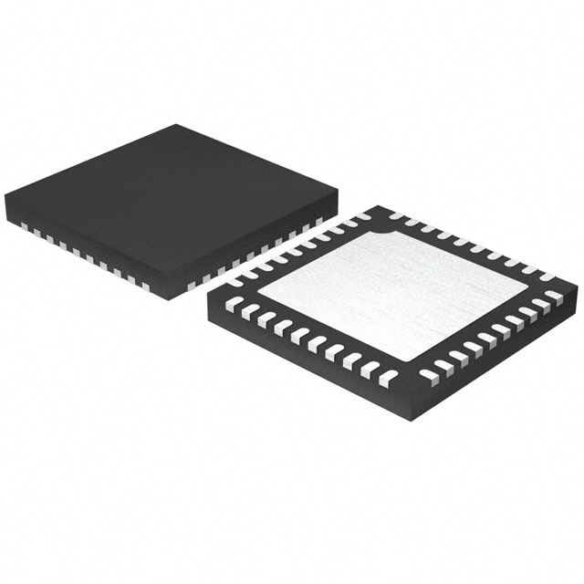
The Skyworks Si53106 is a low-power, six-output differential clock buffer designed for high-speed interconnect applications. It meets Intel DB1200ZL specifications and supports PCIe Gen 1/2/3/4, SAS, SATA, Intel QPI, and Intel SMI. The device operates with a 3.3 V core supply (VDD/VDD_A) and a flexible 1.05 V to 3.3 V I/O supply (VDD_IO). It features an optimized VCO for 100 MHz and 133 MHz inputs, providing low phase jitter compliant with common clock and SRNS standards. The Si53106 offers individual hardware output enables, SMBus programmability for PLL bandwidth and address selection, and operates within an industrial temperature range of –40 °C to 85 °C in a 40-pin QFN package.
Verify the specific ordering suffix against the manufacturer's current guide to ensure correct package and temperature grade. Confirm that the design environment supports the required SMBus logic levels and voltage domains. Ensure proper power filtering components are included as per the datasheet recommendations to maintain signal integrity.
Select this component when distributing reference clocks for Intel QPI, PCIe Gen 1 through Gen 4, SAS, or SATA interfaces. Choose the Si53106 if the design requires independent control of six differential outputs via hardware pins or SMBus. Verify that the input clock frequency matches the selected 100 MHz or 133 MHz optimization point for lowest phase jitter performance.
The Si53106 belongs to Skyworks Solutions' family of zero-delay and buffered clock generators. It is specifically engineered to meet stringent jitter requirements for modern high-speed serial links. The device integrates a PLL optimized for specific frequencies, distinguishing it from general-purpose oscillators by its focus on low-jitter distribution for processor and memory interconnects.
For higher output counts or variations, contact Skyworks Solutions directly. No direct public substitute part numbers are listed in the provided documentation; alternative devices must be evaluated based on pin compatibility, electrical specifications, and application support.
The output frequency is selected via the 100M_133M hardware pin. A logic low selects 133.33 MHz, while a logic high selects 100.00 MHz. The CLK_IN frequency must equal the CLK_OUT frequency.
Yes, the PLL bandwidth can be overridden via SMBus programming using Byte 0 bits 2 and 1. This allows switching between high-bandwidth, bypass, and low-bandwidth modes without changing hardware straps.
Initially, PWRGD samples configuration states like frequency and address. Once asserted high, it functions as PWRDN (Power Down). Asserting PWRDN low shuts off all clocks cleanly in a glitch-free manner before the VCO stops.
 SI53106-A01AGM
The activity of extra discounts on wholesale prices is in full swing…
Please fill in your contact information and we will send you the latest wholesale price list.