 ChipApex | Global Electronic Components Supplier
SEARCH
Search Product
Search Post
— IC芯片 | 连接器 | 传感器 | 被动器件 —
Search productSearch post
— IC芯片 | 连接器 | 传感器 | 被动器件 —
Consult the customer manager about the wholesale price.
consultation hotline:86-132-6715-2157
email:[email protected]
Contact the product manager for consultation. One-stop consultation is available.
Do you want a lower wholesale price? Please send us your inquiry and we will reply immediately.
The SI53159-A01AGM is a nine-output fan-out clock buffer designed for PCIe Gen 1, Gen 2, Gen 3, and Gen 4 applications. It operates with a 3.3 V supply (3.135–3.465 V) and accepts differential inputs from 100 to 210 MHz. The device provides low additive jitter performance, including 0.10 ps RMS phase jitter for PCIe Gen 3 and Gen 4. It features six hardware output enable pins and I2C control capabilities. Packaged in a 48-pin QFN, it supports an extended operating temperature range of –40 to 85 °C.
Verify the specific ordering suffix 'A01AGM' against the manufacturer's current ordering guide to confirm package type and temperature grade. Confirm that the required I2C slave address (D6h) and register map align with the system controller implementation. Ensure PCB land pattern dimensions match the recommended IPC-7351 guidelines for the 48-pin QFN package.
Select this component when a single input clock must be distributed to nine downstream PCIe endpoints with minimal jitter degradation. Verify that the input frequency falls within the 100–210 MHz range. Consider the 48-pin QFN footprint constraints and the need for external termination if not using the internal buffer characteristics. Check if I2C configuration flexibility is required for dynamic output enabling or amplitude adjustment.
The SI53159-A01AGM is part of the Skyworks Si53159 family of PCIe clock buffers. The 'A01AGM' suffix denotes the 48-pin QFN package variant with extended temperature operation (-40 to 85 °C). A tape and reel version, SI53159-A01AGMR, is also available for automated assembly processes.
The SI53159-A01AGMR is the tape and reel equivalent of the SI53159-A01AGM, offering identical electrical and functional specifications but differing only in packaging format for surface-mount assembly.
Outputs can be controlled via six dedicated hardware OE pins (OE_DIFF0 through OE_DIFF3, with others sharing pins) or through the I2C interface by setting the respective DIFFx_OE bits in Control Registers 1 and 2.
It is a dual-function pin. During initial power-up, it acts as CKPWRGD; if low, outputs remain disabled while core logic stays active. Once sampled high, it functions as PDB (Power Down), an active-low asynchronous input that disables all outputs glitch-free.
Yes, via the I2C interface. Byte 5 allows selection of default amplitude or custom amplitude settings ranging from 300 mV to 1000 mV using the DIFF_Amp_Cntl bits.
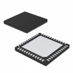 SI53159-A01AGM
The activity of extra discounts on wholesale prices is in full swing…
Please fill in your contact information and we will send you the latest wholesale price list.





