 ChipApex | Global Electronic Components Supplier

SEARCH
Search Product
Search Post
— IC芯片 | 连接器 | 传感器 | 被动器件 —
Search productSearch post
— IC芯片 | 连接器 | 传感器 | 被动器件 —
Consult the customer manager about the wholesale price.
consultation hotline:86-132-6715-2157
email:[email protected]
Contact the product manager for consultation. One-stop consultation is available.
Do you want a lower wholesale price? Please send us your inquiry and we will reply immediately.
SI5330G-B00218-GM is listed in the Clock Buffers, Drivers range at ChipApex. The manufacturer field lists Skyworks Solutions Inc.. Its product description is IC CLK BUFFER 1:8 200MHZ 24QFN. Review the specifications below when checking this part for your BOM.
The SI5330G-B00218-GM is a low-jitter, low-skew clock buffer and level translator from Skyworks Solutions. It accepts a differential input signal and generates eight single-ended CMOS outputs. The device operates with a core supply voltage of 1.8 V, 2.5 V, or 3.3 V, while the output driver supply (VDDO) is set to 2.5 V for this specific part number. It supports input frequencies up to 200 MHz for CMOS outputs. Key electrical characteristics include a typical additive phase jitter of 150 fs RMS (12 kHz–20 MHz), an output-to-output skew of 100 ps, and a typical propagation delay of 2.5 ns. The component is housed in a 24-lead, 4 x 4 mm QFN package.
Verify the ordering suffix against the manufacturer's current documentation to confirm the specific output voltage configuration and shipment media. The base model SI5330G indicates differential input and single-ended CMOS outputs. Confirm whether the 'R' suffix is present for tape-and-reel packaging or absent for tray shipping. Ensure the VDDO supply voltage matches the required 2.5 V specification for this variant during procurement validation.
Select this component when a differential clock source must be fan-out to eight single-ended CMOS loads. The VDDO supply voltage determines the output logic levels; this specific part number is configured for 2.5 V outputs. Ensure the input frequency does not exceed 200 MHz for CMOS operation. Verify that the system requires independent core and output supply voltages, as the Si5330 allows separate VDD and VDDO rails for power optimization.
This part belongs to the Si5330 family of low-jitter clock buffers. The 'G' designation specifically identifies devices with differential inputs and single-ended outputs. Other variants in the family include differential-to-differential buffers (A/B/C) and single-ended-to-differential converters (K/L/M). The Si5330 series is designed for high-performance PCB clock distribution where low skew and jitter are critical requirements.
Direct functional replacements within the same family include SI5330G-B00217-GM (3.3 V CMOS outputs) and SI5330G-B00219-GM (1.8 V CMOS outputs). For different input/output configurations, consider SI5330F-B00218-GMR for single-ended inputs or SI5330C-B00208-GM for differential-to-differential HCSL outputs. Verify pin compatibility and supply voltage requirements before substitution.
Explore related parts through Clock/Timing, Integrated Circuits (ICs), all product categories, ChipApex homepage.
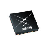 SI5330G-B00218-GM

The activity of extra discounts on wholesale prices is in full swing…
Please fill in your contact information and we will send you the latest wholesale price list.





