 ChipApex | Global Electronic Components Supplier

SEARCH
Search Product
Search Post
— IC芯片 | 连接器 | 传感器 | 被动器件 —
Search productSearch post
— IC芯片 | 连接器 | 传感器 | 被动器件 —
Consult the customer manager about the wholesale price.
consultation hotline:86-132-6715-2157
email:[email protected]
Contact the product manager for consultation. One-stop consultation is available.
Do you want a lower wholesale price? Please send us your inquiry and we will reply immediately.
SI5330H-A00220-GM is listed in the Clock Buffers, Drivers range at ChipApex. The manufacturer field lists Skyworks Solutions Inc.. Its product description is IC CLK BUFFER 1:8 350MHZ 24QFN. Review the specifications below when checking this part for your BOM.
The SI5330H-A00220-GM is a low-jitter, low-skew clock buffer and level translator manufactured by Silicon Laboratories. It accepts differential input signals and generates eight single-ended SSTL outputs. The device operates with a core supply voltage of 1.8 V, 2.5 V, or 3.3 V, while the output driver supply (VDDO) is set to 3.3 V for SSTL compatibility. It supports frequency ranges from 5 MHz to 350 MHz, features an additive jitter of 150 fs RMS typical, and includes a Loss of Signal (LOS) indicator and glitchless Output Enable (OEB) control.
Verify that the ordering suffix matches the required shipment media; adding 'R' specifies tape and reel packaging. Confirm the specific output format configuration code corresponds to the 3.3 V SSTL variant. Ensure the central ground pad is properly connected to the system ground plane during assembly to maintain specified performance.
Select this part when eight single-ended SSTL outputs are required from a differential source. The core supply can be optimized for power consumption at 1.8 V, 2.5 V, or 3.3 V, independent of the 3.3 V output driver supply. Verify that the input signal frequency falls within the 5 MHz to 350 MHz range for SSTL operation.
This component belongs to the Si5330 family of low-jitter clock buffers. The 'H' designation indicates a differential-to-single-ended buffer configuration. Other variants in the series support LVPECL, LVDS, HCSL, CMOS, and HSTL formats with varying input types.
Other Si5330 variants such as SI5330G-A00219-GM provide similar functionality but with different output voltage levels or signal formats. Direct substitution requires matching the output drive strength and voltage requirements of the downstream circuitry.
The LOS pin is an open-drain output that indicates the status of the input clock. It asserts low when a valid clock signal is present and goes high when a loss of signal is detected.
The Output Enable (OEB) pin allows glitchless control of the output clocks. Connecting it to ground enables all outputs, while connecting it to VDD disables them, forcing outputs to a logic low state.
The center ground pad must be tied to the system ground using no less than five vias to a ground plane located no more than 20 mils below to ensure proper thermal dissipation and electrical performance.
Explore related parts through Clock/Timing, Integrated Circuits (ICs), all product categories, ChipApex homepage.
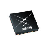 SI5330H-A00220-GM

The activity of extra discounts on wholesale prices is in full swing…
Please fill in your contact information and we will send you the latest wholesale price list.





