 ChipApex | Global Electronic Components Supplier

SEARCH
Search Product
Search Post
— IC芯片 | 连接器 | 传感器 | 被动器件 —
Search productSearch post
— IC芯片 | 连接器 | 传感器 | 被动器件 —
Consult the customer manager about the wholesale price.
consultation hotline:86-132-6715-2157
email:[email protected]
Contact the product manager for consultation. One-stop consultation is available.
Do you want a lower wholesale price? Please send us your inquiry and we will reply immediately.
SI53328-B-GM is listed in the Clock Buffers, Drivers range at ChipApex. The manufacturer field lists Skyworks Solutions Inc.. Its product description is IC CLK BUFFER 2:6 200MHZ 24QFN. Review the specifications below when checking this part for your BOM.
The Skyworks SI53328-B-GM is a low-jitter LVPECL fanout clock buffer featuring a 2:1 selectable input multiplexer and two independent output banks. It accepts single-ended LVCMOS inputs and provides up to three LVPECL outputs per bank, totaling six outputs. The device operates from DC to 200 MHz with a typical additive jitter of 50 fs rms. Built-in LDOs deliver high power supply noise rejection (PSRR), reducing external filtering requirements. It supports independent output enables for each bank and functions within a supply voltage range of 2.38–2.63 V or 2.97–3.63 V.
Verify the specific ordering suffix against the manufacturer's current datasheet to confirm package type and temperature range. Ensure the design accommodates the 24-QFN footprint dimensions of 4 x 4 mm. Confirm that the application requires single-ended LVCMOS inputs, as this variant does not support universal differential inputs.
Select the SI53328-B-GM when dual-bank redundancy with independent control is required alongside single-ended LVCMOS input compatibility. This part is distinct from the Si53327, which supports universal any-format inputs. Ensure the target frequency remains within the 200 MHz limit specified for this model.
This component belongs to the Si53320–28 family of low-jitter LVPECL fanout buffers. While other members like the Si53327 offer universal input formats, the Si53328 is specifically configured for single-ended LVCMOS inputs. It shares the same 24-QFN package and dual-bank architecture as its sibling but differs in input interface capabilities.
The Si53327-B-GM is a functional alternative if universal input support (LVDS, CML, etc.) is needed instead of LVCMOS-only. Both share the 24-QFN package and dual-bank structure. Verify input signal compatibility before substitution.
Explore related parts through Clock/Timing, Integrated Circuits (ICs), all product categories, ChipApex homepage.
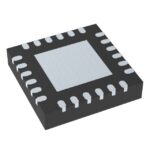 SI53328-B-GM

The activity of extra discounts on wholesale prices is in full swing…
Please fill in your contact information and we will send you the latest wholesale price list.





