 ChipApex | Global Electronic Components Supplier

SEARCH
Search Product
Search Post
— IC芯片 | 连接器 | 传感器 | 被动器件 —
Search productSearch post
— IC芯片 | 连接器 | 传感器 | 被动器件 —
Consult the customer manager about the wholesale price.
consultation hotline:86-132-6715-2157
email:[email protected]
Contact the product manager for consultation. One-stop consultation is available.
Do you want a lower wholesale price? Please send us your inquiry and we will reply immediately.
SI53345-B-GMR is listed in the Clock Buffers, Drivers range at ChipApex. The manufacturer field lists Skyworks Solutions Inc.. Its product description is IC CLK BUFFER 2:10 200MHZ 32QFN. Review the specifications below when checking this part for your BOM.
The Skyworks SI53345-B-GMR is a low-jitter LVDS fanout buffer featuring ten differential LVDS outputs. It accepts single-ended LVCMOS inputs and operates over a frequency range from DC to 200 MHz. The device includes a 2:1 input multiplexer for selecting between two clock sources, controlled by the CLK_SEL pin. Built-in LDOs provide high power supply noise rejection (PSRR), reducing external filtering requirements. It supports independent output enable controls and functions within an ambient temperature range of –40 °C to +85 °C.
Verify the specific ordering suffix matches the required package and tape/reel configuration. Confirm that the LVCMOS-only input variant aligns with the source signal format, as universal input models exist within the family. Ensure thermal management meets the junction temperature limits specified in the datasheet.
Select this model when ten LVDS outputs are required from a single-ended LVCMOS source. For applications needing universal input formats like LVPECL or LVDS, choose the SI53344 variant instead. Verify that the 200 MHz maximum frequency meets system requirements, as other family members support up to 1250 MHz.
This component belongs to the Si53340-45 family of low-jitter LVDS fanout buffers. The family differentiates models by input format (universal vs. LVCMOS) and output count (4, 3, or 10). The SI53345 specifically targets LVCMOS inputs with a full bank of ten outputs.
SI53344-B-GM provides identical ten-output LVDS capability but accepts any-format inputs including LVDS and LVPECL.
Explore related parts through Clock/Timing, Integrated Circuits (ICs), all product categories, ChipApex homepage.
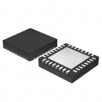 SI53345-B-GMR

The activity of extra discounts on wholesale prices is in full swing…
Please fill in your contact information and we will send you the latest wholesale price list.




