 ChipApex | Global Electronic Components Supplier

SEARCH
Search Product
Search Post
— IC芯片 | 连接器 | 传感器 | 被动器件 —
Search productSearch post
— IC芯片 | 连接器 | 传感器 | 被动器件 —
Consult the customer manager about the wholesale price.
consultation hotline:86-132-6715-2157
email:[email protected]
Contact the product manager for consultation. One-stop consultation is available.
Do you want a lower wholesale price? Please send us your inquiry and we will reply immediately.
SI53365-B-GT is listed in the Clock Buffers, Drivers range at ChipApex. The manufacturer field lists Skyworks Solutions Inc.. Its product description is IC CLK BUFFER 1:8 200MHZ 16TSSOP. Review the specifications below when checking this part for your BOM.
The Skyworks Solutions Inc. Si53365-B-GT is a low-jitter, LVCMOS fanout clock buffer featuring eight outputs and a frequency range from DC to 200 MHz. Utilizing advanced CMOS technology, it guarantees low additive jitter of 120 fs RMS, low skew, and minimal propagation delay variability. The device integrates built-in LDOs for high PSRR performance, eliminating the need for external filtering components. It operates within an ambient temperature range of –40 °C to +85 °C and supports supply voltages of 1.8 V, 2.5 V, or 3.3 V.
Verify the specific ordering suffix '-GT' against the manufacturer's current datasheet to confirm package type and tape-and-reel specifications. Confirm RoHS compliance status via the official Skyworks Certificate of Conformance before procurement.
Select the Si53365 variant specifically for single-ended LVCMOS input requirements. Ensure the application does not require dual-input multiplexing, which is available in the Si53360/61/62 family. Validate that the load capacitance and slew rate requirements align with the AC characteristics defined in the electrical specifications table.
The Si53365 belongs to the Si5336x family of fixed-format LVCMOS buffers. Unlike the Si53360/61/62 models, it features a single clock input rather than a dual-input MUX configuration. It provides eight outputs, whereas the Si53362 offers twelve outputs split into two banks.
Publicly confirmed substitute part numbers are not available in the provided documentation. Verify pin compatibility and electrical parameters if considering alternative manufacturers.
No, the Si53365 features a single clock input (CLK). Dual-input MUX functionality is available in the Si53360, Si53361, and Si53362 models.
The device guarantees a typical low additive jitter of 120 fs RMS, measured from 12 kHz to 20 MHz.
Unused outputs should be left unconnected to ensure proper operation and minimize noise coupling.
Explore related parts through Clock/Timing, Integrated Circuits (ICs), all product categories, ChipApex homepage.
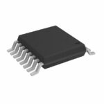 SI53365-B-GT

The activity of extra discounts on wholesale prices is in full swing…
Please fill in your contact information and we will send you the latest wholesale price list.




