 ChipApex | Global Electronic Components Supplier
SEARCH
Search Product
Search Post
— IC芯片 | 连接器 | 传感器 | 被动器件 —
Search productSearch post
— IC芯片 | 连接器 | 传感器 | 被动器件 —
Consult the customer manager about the wholesale price.
consultation hotline:86-132-6715-2157
email:[email protected]
Contact the product manager for consultation. One-stop consultation is available.
Do you want a lower wholesale price? Please send us your inquiry and we will reply immediately.
The SI5338A-B04774-GM is a programmable quad clock generator utilizing MultiSynth technology. It synthesizes any frequency on four independent outputs with zero ppm precision. The device supports differential and single-ended formats including LVPECL, LVDS, CML, HCSL, CMOS, SSTL, and HSTL. Maximum output frequencies reach 710 MHz for differential signals and 200 MHz for CMOS. It operates from a 1.8 V, 2.5 V, or 3.3 V core supply with typical current consumption of 45 mA. Integrated phase jitter is typically 0.7 ps RMS.
Verify the specific ordering suffix against the manufacturer's official documentation to confirm pinout compatibility and factory configuration. Ensure the I2C pull-up voltage aligns with the system bus requirements, as register adjustments may be necessary for voltages below 2.5 V. Confirm package integrity upon receipt, as the component is moisture sensitive.
Select this model for applications requiring high-precision clock synthesis across multiple domains. Ensure the required output format matches the supported voltage ranges (1.5 V, 1.8 V, 2.5 V, or 3.3 V). Verify that the input reference source falls within the specified frequency limits for the chosen interface type. Utilize ClockBuilder Pro software for optimal configuration and jitter performance validation.
This component belongs to the Si5338 family of I2C-programmable clock generators. It replaces discrete crystal oscillators by providing four independent clock outputs from a single reference. The device integrates a PLL and MultiSynth synthesizers to achieve low-jitter performance in a compact 4x4 mm QFN package suitable for space-constrained designs.
Direct replacements must maintain the same pinout and functional capabilities. Consult the manufacturer's cross-reference guide for verified substitutes. Ensure alternative components support the required output formats and frequency ranges without compromising jitter specifications.
The maximum differential output frequency is 710 MHz for LVPECL, LVDS, and CML formats.
Yes, the Si5338 supports a clock buffer mode (PLL bypass) where the input clock is directly passed to the outputs.
The device is programmed via an I2C/SMBus-compatible serial interface using registers accessible through SCL and SDA pins.
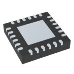 SI5338A-B04774-GM
The activity of extra discounts on wholesale prices is in full swing…
Please fill in your contact information and we will send you the latest wholesale price list.







