ChipApex | Global Electronic Components Supplier

SEARCH
Search Product
Search Post
— IC芯片 | 连接器 | 传感器 | 被动器件 —
Search productSearch post
— IC芯片 | 连接器 | 传感器 | 被动器件 —
Consult the customer manager about the wholesale price.
consultation hotline:86-132-6715-2157
email:[email protected]
Contact the product manager for consultation. One-stop consultation is available.
Do you want a lower wholesale price? Please send us your inquiry and we will reply immediately.
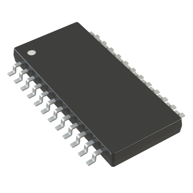
SI5351C-A-GU is listed in the Clock Generators, PLLs, Frequency Synthesizers range at ChipApex. The manufacturer field lists Skyworks Solutions Inc.. Its product description is IC CLOCK GENERATOR 24QSOP. Review the specifications below when checking this part for your BOM.
The SI5351C-A-GU is an I2C-programmable CMOS clock generator from Silicon Labs, designed to replace crystals, oscillators, and PLLs. It generates up to eight non-integer-related frequencies ranging from 8 kHz to 160 MHz with 0 ppm error using a PLL/MultiSynth architecture. The device synchronizes to an external reference clock (CLKIN) inputting 10–100 MHz. It features separate core (VDD: 2.5/3.3 V) and output (VDDO: 1.8/2.5/3.3 V) supplies, low period jitter (100 ps pk-pk typical), and configurable spread spectrum. Packaged in a 24-QSOP, it supports glitchless frequency changes and static phase offsets.
Verify the specific package type and operating temperature range against the datasheet specifications before procurement. Confirm that the external reference clock signal levels are compatible with the CLKIN input requirements. Ensure proper decoupling capacitors are placed near the VDD and VDDO pins to maintain signal integrity and power supply stability during operation.
Select this model when synchronization to an external clock source is required rather than free-running generation. Compare the 24-QSOP package dimensions against board space constraints relative to QFN or MSOP alternatives. Evaluate the need for multiple independent voltage domains if different output logic levels are necessary for downstream components.
This component belongs to the Si5351 family of clock generators. The 'C' variant specifically denotes support for an external clock input (CLKIN). The 'A' suffix indicates standard performance characteristics without factory-customized EMI profiles. The 'GU' suffix identifies the 24-pin QSOP package option within the product line.
Si5351C-B-GM
The device can generate output frequencies up to 160 MHz.
It synchronizes to an external reference clock applied to the CLKIN pin, which accepts frequencies between 10 MHz and 100 MHz.
Yes, separate output supply pins (VDDO) allow each bank of outputs to operate at 1.8 V, 2.5 V, or 3.3 V.
Explore related parts through Clock/Timing, Integrated Circuits (ICs), all product categories, ChipApex homepage.
 SI5351C-A-GU

The activity of extra discounts on wholesale prices is in full swing…
Please fill in your contact information and we will send you the latest wholesale price list.