 ChipApex | Global Electronic Components Supplier
SEARCH
Search Product
Search Post
— IC芯片 | 连接器 | 传感器 | 被动器件 —
Search productSearch post
— IC芯片 | 连接器 | 传感器 | 被动器件 —
Consult the customer manager about the wholesale price.
consultation hotline:86-132-6715-2157
email:[email protected]
Contact the product manager for consultation. One-stop consultation is available.
Do you want a lower wholesale price? Please send us your inquiry and we will reply immediately.
The SiTime SIT92110AI-Y is a 10-output low-jitter clock fan-out buffer designed for high-frequency clock distribution. It features a 3:1 input multiplexer supporting primary, secondary, or crystal sources with LVCMOS outputs. The device operates on independent core (VDD) and output (VDDO) supplies ranging from 1.5 V to 3.3 V. Key electrical parameters include an additive jitter of 50 fs RMS, typical output skew of 30 ps, and a maximum frequency of 250 MHz. It is housed in a 32-pin 5 mm x 5 mm QFN package.
Verify the ordering suffix 'Y' corresponds to the tape and reel packaging configuration as defined in the manufacturer's ordering guide. Confirm that the specific revision level matches the design requirements. Ensure supply voltage domains align with the specified VDD and VDDO ranges before procurement.
Select this component when ten LVCMOS outputs are required from a single clock source. Ensure the input signal meets the minimum slew rate requirement of 2 V/ns for optimal jitter performance. Verify that the target load impedance and termination strategy match the driver capabilities at the chosen VDDO voltage.
The SIT92110 belongs to the SiT92xxx series of clock buffers. It provides a solution for distributing a single reference clock to multiple downstream components while maintaining signal integrity. The device supports flexible input selection via pin strapping, allowing adaptation to various system architectures.
Parameter equivalent alternatives include SIT92110AI-T and SIT92110AI-X. These variants share identical electrical specifications but differ in packaging format. Verify compatibility with existing PCB footprints and reflow profiles when substituting.
The maximum output frequency is 250 MHz for universal clock inputs and 50 MHz when driven by a crystal oscillator.
Pulling the OE pin LOW forces outputs to a high-impedance state after four falling edges of the input signal. Pulling OE HIGH enables the outputs.
Yes, the XTAL_IN pin can be overdriven with a single-ended clock signal up to 250 MHz in crystal bypass mode, provided the peak swing does not exceed 1.8 V.
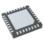 SIT92110AI-Y
The activity of extra discounts on wholesale prices is in full swing…
Please fill in your contact information and we will send you the latest wholesale price list.





