 ChipApex | Global Electronic Components Supplier

SEARCH
Search Product
Search Post
— IC芯片 | 连接器 | 传感器 | 被动器件 —
Search productSearch post
— IC芯片 | 连接器 | 传感器 | 被动器件 —
Consult the customer manager about the wholesale price.
consultation hotline:86-132-6715-2157
email:[email protected]
Contact the product manager for consultation. One-stop consultation is available.
Do you want a lower wholesale price? Please send us your inquiry and we will reply immediately.
SIT92211AI-N is listed in the Clock Buffers, Drivers range at ChipApex. The manufacturer field lists SiTime. Its product description is -40C TO 85C, 48PIN, 7070, 1.8V-3. Review the specifications below when checking this part for your BOM.
The SiTime SIT92211AI-N is a 2.1 GHz, 10-output ultra-low jitter clock fan-out buffer designed for high-frequency clock distribution and level translation. It features three selectable clock inputs: two universal differential or single-ended inputs (CLKin0/1) supporting up to 2.1 GHz, and one crystal input (OSCIN) for 8 MHz to 50 MHz crystals or single-ended clocks. The device distributes the selected clock to two independent output driver banks (A and B), each providing five differential outputs, plus one synchronized LVCMOS reference output (REFOUT). Output drivers can be independently configured as LVPECL, LVDS, HCSL, or Hi-Z. The core supply operates at 3.3 V or 2.5 V, while differential outputs support 3.3 V or 2.5 V, and the LVCMOS output supports 3.3 V, 2.5 V, or 1.8 V.
Verify the specific ordering suffix 'N' against the manufacturer's official documentation to confirm package type and tape/reel specifications. Ensure the required output voltage levels (3.3 V, 2.5 V, or 1.8 V) match the system design constraints for both core and output supplies.
Select this component when applications require distributing a high-frequency clock signal (>1 GHz) with minimal added jitter. Consider the available input types (differential vs. single-ended/crystal) and the required output logic families (LVPECL, LVDS, HCSL, LVCMOS). Verify that the PCB layout can accommodate the 48-pin QFN package and proper thermal dissipation.
The SIT92211 belongs to SiTime's high-performance clock buffer family, specifically engineered for demanding digital systems. It replaces traditional quartz-based buffers by offering lower jitter, smaller form factors, and greater flexibility in input/output configurations. The AI suffix typically denotes an industrial temperature range (-40°C to 85°C) and specific quality grades.
Direct pin-to-pin replacements may not exist due to the specific 48-pin QFN footprint and unique control pin configuration. Evaluate other SiTime models like the SiT92216 or SiT92315 if pin count or output configuration differs. Cross-check electrical parameters such as maximum frequency and jitter specs before substituting.
The SiT92211 accepts two universal clock inputs (CLKin0/1) which can be differential or single-ended, operating up to 2.1 GHz. It also has a dedicated crystal input (OSCIN) for crystals between 8 MHz and 50 MHz or single-ended clocks.
No, the output drivers in Bank A and Bank B must be configured uniformly. Each bank can be set to LVPECL, LVDS, HCSL, or Hi-Z mode via control pins, but all outputs within a single bank share the same configuration.
The LVCMOS output (REFOUT) is synchronized to the selected clock input. It can be enabled or disabled in a glitch-free manner using the REFOUT_EN pin, ensuring clean transitions during state changes.
Explore related parts through Clock/Timing, Integrated Circuits (ICs), all product categories, ChipApex homepage.
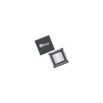 SIT92211AI-N

The activity of extra discounts on wholesale prices is in full swing…
Please fill in your contact information and we will send you the latest wholesale price list.




