 ChipApex | Global Electronic Components Supplier

SEARCH
Search Product
Search Post
— IC芯片 | 连接器 | 传感器 | 被动器件 —
Search productSearch post
— IC芯片 | 连接器 | 传感器 | 被动器件 —
Consult the customer manager about the wholesale price.
consultation hotline:86-132-6715-2157
email:[email protected]
Contact the product manager for consultation. One-stop consultation is available.
Do you want a lower wholesale price? Please send us your inquiry and we will reply immediately.
SIT92211AI-T is listed in the Clock Buffers, Drivers range at ChipApex. The manufacturer field lists SiTime. Its product description is -40C TO 85C, 48PIN, 7070, 1.8V-3. Review the specifications below when checking this part for your BOM.
The SiTime SIT92211AI-T is a 10-output, differential ultra-low jitter clock fan-out buffer designed for high-frequency clock distribution and level translation. It supports input frequencies up to 2.1 GHz with an additive jitter performance of 55 fs RMS. The device features three selectable clock inputs: two universal inputs (CLKin0/1) accepting LVPECL, LVDS, LVCMOS, CML, HCSL, SSTL, or single-ended clocks, and one crystal input supporting 8 MHz to 50 MHz crystals. Outputs are distributed across two programmable differential banks (A and B) and one LVCMOS output (REFOUT). Differential outputs support LVPECL, LVDS, HCSL, or Hi-Z modes, while the LVCMOS output operates at 1.8 V, 2.5 V, or 3.3 V. The component operates from 3.3 V/2.5 V core and output supplies within a -40°C to 85°C temperature range.
Verify the ordering suffix 'T' corresponds to the tape-and-reel packaging configuration as specified in the manufacturer's documentation. Confirm that the 'AI' suffix aligns with the required industrial temperature range (-40°C to 85°C) and voltage specifications. Ensure compatibility with the 48-pin QFN package dimensions for PCB layout. Cross-reference the specific part number against current distributor listings to confirm availability and lead times, as stock levels may vary.
Select this component when designing systems requiring a 3:1 input mux with support for both differential and single-ended sources up to 2.1 GHz. It is suitable for applications needing simultaneous level translation between 3.3 V/2.5 V domains and 1.8 V LVCMOS logic. Consider the power supply requirements: separate VCCO supplies for Bank A, Bank B, and the LVCMOS output allow for independent voltage scaling. Ensure the application can accommodate the 48-pin 7mm x 7mm QFN package footprint and thermal dissipation needs.
The SIT92211 belongs to the SiT92xxx series of high-performance clock buffers. It is distinct from lower-output variants like the SiT9211x series, which offer fewer outputs and smaller packages. This specific model provides a comprehensive solution for complex clock trees requiring multiple differential outputs and a reference clock, differentiating it from simpler fan-out buffers or oscillators.
Direct parameter-equivalent substitutes include other SiTime models within the SIT92211 family with different packaging or temperature suffixes, such as SIT92211AI-X or SIT92211AI-Y. Verify pinout compatibility and electrical characteristics before substitution.
The universal clock inputs (CLKin0 and CLKin1) support LVPECL, LVDS, LVCMOS, CML (AC-coupled only), HCSL, SSTL, and single-ended clocks.
Yes, the OSCIN pin can accept a single-ended clock signal in bypass mode or be over-driven by an AC-coupled single-ended clock in crystal over-drive mode.
The SiT92211 supports input and output frequencies up to 2.1 GHz.
Explore related parts through Clock/Timing, Integrated Circuits (ICs), all product categories, ChipApex homepage.
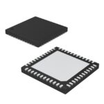 SIT92211AI-T

The activity of extra discounts on wholesale prices is in full swing…
Please fill in your contact information and we will send you the latest wholesale price list.






