 ChipApex | Global Electronic Components Supplier

SEARCH
Search Product
Search Post
— IC芯片 | 连接器 | 传感器 | 被动器件 —
Search productSearch post
— IC芯片 | 连接器 | 传感器 | 被动器件 —
Consult the customer manager about the wholesale price.
consultation hotline:86-132-6715-2157
email:[email protected]
Contact the product manager for consultation. One-stop consultation is available.
Do you want a lower wholesale price? Please send us your inquiry and we will reply immediately.
SIT92211AI-X is listed in the Clock Buffers, Drivers range at ChipApex. The manufacturer field lists SiTime. Its product description is -40C TO 85C, 48PIN, 7070, 1.8V-3. Review the specifications below when checking this part for your BOM.
The SiT92211 is a 2.1 GHz, 10-output ultra-low jitter clock fan-out buffer designed for high-frequency clock distribution and level translation. It features two universal differential or single-ended inputs supporting up to 2.1 GHz, one crystal input (8–50 MHz), and one LVCMOS reference output. The device provides ten outputs across two banks (A and B) configurable as LVPECL, LVDS, HCSL, or Hi-Z. Additive jitter is typically 55 fs RMS. It operates with core supplies of 3.3 V or 2.5 V, output supplies of 3.3 V/2.5 V, and an LVCMOS supply of 1.8 V/2.5 V/3.3 V. The component is housed in a 48-pin, 7 mm x 7 mm QFN package.
Verify the specific ordering suffix against the manufacturer's current datasheet to confirm voltage options and package variants. Ensure that the design accounts for the required external termination resistors for LVPECL, LVDS, and HCSL modes. Confirm power supply sequencing and decoupling requirements for the multiple VCCO domains to maintain signal integrity.
Select this component when distributing clocks to mixed-voltage logic families such as LVPECL, LVDS, and LVCMOS simultaneously. The dual-bank architecture allows independent configuration of output drive types. Verify that the input source matches the supported formats (differential/single-ended/crystal) and that the frequency does not exceed 2.1 GHz for full swing operation.
The SiT92211 belongs to SiTime’s high-performance clock buffer family, specifically engineered for applications demanding minimal added jitter. It serves as a replacement for traditional discrete buffer solutions by integrating multiple output standards and input selection into a single surface-mount package, simplifying PCB layout and reducing component count.
Publicly confirmed substitute part numbers are not available in the provided documentation. Designers should consult the manufacturer's official cross-reference tools or contact sales representatives for validated alternatives compatible with the 48-pin QFN form factor and electrical specifications.
The SiT92211 supports LVPECL, LVDS, HCSL, and High-Impedance (Hi-Z) modes for its differential output banks. The dedicated reference output supports LVCMOS levels.
Yes, the two universal clock inputs (CLKin0 and CLKin1) can accept single-ended signals. Additionally, the OSCIN pin can accept a single-ended clock in bypass mode.
The crystal input supports crystals with frequencies ranging from 8 MHz to 50 MHz. In bypass mode, it can accept an external single-ended clock up to 250 MHz.
Explore related parts through Clock/Timing, Integrated Circuits (ICs), all product categories, ChipApex homepage.
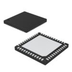 SIT92211AI-X

The activity of extra discounts on wholesale prices is in full swing…
Please fill in your contact information and we will send you the latest wholesale price list.





