 ChipApex | Global Electronic Components Supplier

SEARCH
Search Product
Search Post
— IC芯片 | 连接器 | 传感器 | 被动器件 —
Search productSearch post
— IC芯片 | 连接器 | 传感器 | 被动器件 —
Consult the customer manager about the wholesale price.
consultation hotline:86-132-6715-2157
email:[email protected]
Contact the product manager for consultation. One-stop consultation is available.
Do you want a lower wholesale price? Please send us your inquiry and we will reply immediately.
SL18860DCT is listed in the Clock Buffers, Drivers range at ChipApex. The manufacturer field lists Skyworks Solutions Inc.. Its product description is IC CLK BUFFER 1:3 52MHZ 10TDFN. Review the specifications below when checking this part for your BOM.
The SL18860DCT is a 3-channel clock distribution buffer manufactured by Silicon Laboratories Inc. It provides three single-ended LVCMOS outputs from a single input, supporting frequencies from 10MHz to 52MHz. The device operates on a 1.7V to 3.65V supply and features ultra-low phase noise and low current consumption (typical 2.7mA at 1.8V). Each output has independent enable control via OE1/2/3 pins to minimize power usage. Packaged in a 10-pin TDFN (1.4x2.0x0.75 mm), it supports industrial temperatures (-40°C to 85°C) and includes an OE_OSC pin for external oscillator control.
Verify the 'DCT' suffix indicates Tape and Reel shipping format versus the standard Tube packaging for the base part number. Confirm the component is sourced from Silicon Laboratories Inc., as indicated in the datasheet header, despite the Skyworks brand query. Ensure the specific revision (Rev 2.0) matches design requirements.
Select this component for designs requiring low-power clock buffering with independent channel control. Verify that the load capacitance requirements (max 20pF typ) align with the driven circuits. Note that the datasheet explicitly marks this device as 'Not Recommended for New Designs,' suggesting evaluation of newer alternatives for future projects.
This component belongs to the SL18860 family of clock buffers. The 'DC' denotes the 10-pin TDFN package variant, while 'DCT' specifies the tape and reel shipping configuration. It is designed to isolate devices driven by clock outputs to minimize interference in mobile RF applications like WLAN and Bluetooth.
The datasheet explicitly states 'Not Recommended for New Designs.' Engineers should consult Silicon Laboratories for updated timing portfolio recommendations or compatible successor components before finalizing a design.
The OE_OSC pin controls the external TCXO/XO. It outputs a logic low (0) only when all three output enables (OE1, OE2, OE3) are low; otherwise, it outputs high.
When all output enables (OE1/2/3) are set to 0, the device enters a standby mode with maximum operating supply current of 1.0µA to 2.0µA depending on VDD.
The maximum load capacitance (CL) for CLKOUT1/2/3 is specified as 20pF typical and 25pF maximum depending on the supply voltage conditions.
Explore related parts through Clock/Timing, Integrated Circuits (ICs), all product categories, ChipApex homepage.
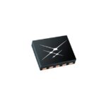 SL18860DCT

The activity of extra discounts on wholesale prices is in full swing…
Please fill in your contact information and we will send you the latest wholesale price list.




