 ChipApex | Global Electronic Components Supplier

SEARCH
Search Product
Search Post
— IC芯片 | 连接器 | 传感器 | 被动器件 —
Search productSearch post
— IC芯片 | 连接器 | 传感器 | 被动器件 —
Consult the customer manager about the wholesale price.
consultation hotline:86-132-6715-2157
email:[email protected]
Contact the product manager for consultation. One-stop consultation is available.
Do you want a lower wholesale price? Please send us your inquiry and we will reply immediately.
SL2305SI-1H is listed in the Clock Generators, PLLs, Frequency Synthesizers range at ChipApex. The manufacturer field lists Skyworks Solutions Inc.. Its product description is IC BUFFER 140MHZ 5CH 3.3V 8SOIC. Review the specifications below when checking this part for your BOM.
The SL2305SI-1H is a low skew, low jitter Zero Delay Buffer (ZDB) manufactured by Silicon Laboratories Inc. It generates up to five clock outputs from one reference input for high-speed distribution applications. The -1H suffix denotes the High-Drive version, supporting frequencies up to 140 MHz with a 15 pF load. Operating on a 3.3 V supply, it consumes 14 mA at 66 MHz and 26 mA at 133 MHz. Key electrical parameters include a maximum cycle-to-cycle jitter of 140 ps at 66 MHz, output-to-output skew of 150 ps, and product-to-product skew of 400 ps. It features SpreadThru™ PLL technology and enters power-down mode if the input is DC.
Verify that the component is sourced from authorized distributors or direct manufacturer channels to ensure authenticity. Confirm the specific package type matches the design requirements, as the device is available in both SOIC and TSSOP formats. Check for RoHS compliance status and verify the temperature grade corresponds to the intended operating environment before finalizing procurement.
Select the -1H variant when driving higher capacitance loads or requiring frequencies up to 140 MHz. Use the standard drive version for lower frequency applications up to 100 MHz to optimize EMI performance. Ensure all clock outputs are loaded equally to maintain specified skew values. Verify that the application does not require new designs, as this part is marked Not Recommended for New Designs.
This component belongs to the SL2305 family of Zero Delay Buffers produced by Silicon Laboratories Inc. It is designed for clock distribution in digital systems requiring precise timing alignment. The device integrates an on-chip PLL that locks to the input clock and provides internal feedback via the CLKOUT pin to minimize delay between input and outputs.
Refer to the SL23EP05 for extended frequency operation ranging from 10 to 220 MHz and a wider power supply range of 2.5V to 3.3V. Evaluate alternative devices within the same family based on required drive strength and package configuration.
If the input at CLKIN is DC (0 to VDD), the device detects this condition and forces all five outputs to a high-impedance state while turning off the PLL, resulting in a power consumption of less than 12 μA.
The CLKOUT pin serves as a buffered clock output and is used internally for feedback to the PLL. Adjusting the load capacitance on this pin relative to other outputs allows for zero-delay adjustment between the input and outputs.
Yes, the device features SpreadThru™ PLL technology, which allows it to pass modulated Spread Spectrum Clock signals from the input to the outputs without degrading the spread percentage, profile, or modulation frequency.
Explore related parts through Clock/Timing, Integrated Circuits (ICs), all product categories, ChipApex homepage.
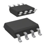 SL2305SI-1H

The activity of extra discounts on wholesale prices is in full swing…
Please fill in your contact information and we will send you the latest wholesale price list.





