 ChipApex | Global Electronic Components Supplier

SEARCH
Search Product
Search Post
— IC芯片 | 连接器 | 传感器 | 被动器件 —
Search productSearch post
— IC芯片 | 连接器 | 传感器 | 被动器件 —
Consult the customer manager about the wholesale price.
consultation hotline:86-132-6715-2157
email:[email protected]
Contact the product manager for consultation. One-stop consultation is available.
Do you want a lower wholesale price? Please send us your inquiry and we will reply immediately.
SL28PCIE14ALI is listed in the Application Specific Clock/Timing range at ChipApex. The manufacturer field lists Skyworks Solutions Inc.. Its product description is IC CLOCK PCIE GEN2/3 BUFF 32QFN. Review the specifications below when checking this part for your BOM.
The SL28PCIe14ALI is a PCI-Express Gen 2 & Gen 3 compliant clock generator and fan-out buffer utilizing EProClock® technology. It features four low-power push-pull differential output buffers with integrated resistors, operating at frequencies up to 100 MHz. The device supports a 25 MHz crystal or clock input and offers hardware-selectable buffered input or synthesizer modes. Key specifications include a 3.3V power supply, industrial temperature range (-40°C to 85°C), and SMBus programmability for frequency and spread spectrum control.
Verify the specific ordering suffix against the datasheet table on page 12. The 'I' suffix denotes Industrial temperature range (-40°C to 85°C), while 'C' indicates Commercial range. The 'T' suffix specifies Tape and Reel packaging; absence of 'T' implies Tube packaging. Confirm package type is 32-pin QFN (5x5mm).
Select based on required temperature range and packaging format. Ensure the input source matches either a 25MHz crystal or a 3.3V CMOS clock signal. Verify that the target application requires the specific jitter performance metrics defined for PCIe Gen 2/3 compliance, particularly the RMS phase jitter limits under specified PLL bandwidth conditions.
This component belongs to the Skyworks SL28PCIe family of clock generators. It is distinct from other models in the series by its specific combination of four differential outputs, EProClock® programmability, and support for both synthesizer and fan-out buffer modes within a single 32-pin QFN package.
Direct replacements must match the 32-pin QFN footprint and pinout. Consider Skyworks models such as SL28PCIe16ALIT or SL28PCIe26ALCT if higher output counts or different input configurations are acceptable, provided they meet the same PCIe Gen 2/3 electrical specifications.
The Spread Spectrum profile is selected using the SS1 and SS0 pins. Logic levels applied to these pins before CKPWRGD assertion determine the modulation percentage (OFF, -0.5%, +/-0.25%, or -0.75%).
It is a dual-function pin. During power-up, it acts as CKPWRGD to latch inputs. Once sampled HIGH, it functions as PD#, an asynchronous active-LOW input used to cleanly shut off all clocks before power removal.
Yes. By setting IN_SEL high, the device operates in Fan-out Buffer mode, accepting an external differential serial reference clock input on DIFFIN/DIFFIN# instead of using the internal synthesizer with a crystal.
Explore related parts through Clock/Timing, Integrated Circuits (ICs), all product categories, ChipApex homepage.
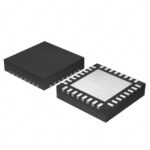 SL28PCIE14ALI

The activity of extra discounts on wholesale prices is in full swing…
Please fill in your contact information and we will send you the latest wholesale price list.






