ChipApex | Global Electronic Components Supplier
SLG59M1571V
Search Product
Search Post
— IC芯片 | 连接器 | 传感器 | 被动器件 —
Search productSearch post
— IC芯片 | 连接器 | 传感器 | 被动器件 —
Consult the customer manager about the wholesale price.
consultation hotline:86-132-6715-2157
email:[email protected]
Contact the product manager for consultation. One-stop consultation is available.
Do you want a lower wholesale price? Please send us your inquiry and we will reply immediately.
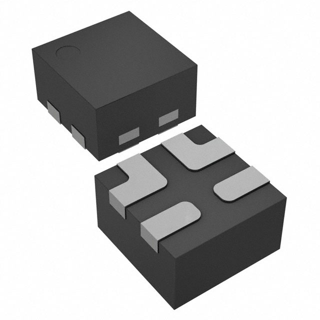
The SLG59M1571V is a single N-channel reverse blocking load switch designed for high-side power control in low-voltage applications. It features a 14.6mΩ typical on-resistance and supports a continuous current of 1A. The device operates within an input voltage range of 0.85V to 1.9V, with a maximum supply voltage of 1.9V. Key electrical parameters include a maximum quiescent current of 27µA when active and 3µA when off. It provides over-temperature protection and output discharge functionality. The component is housed in a compact 1.0mm x 1.0mm STDFN-4 package.
Verify the specific ordering suffix corresponds to the required tape and reel configuration, such as standard reel or cut tape options. Confirm that the application voltage does not exceed the 1.9V maximum rating. Ensure thermal design accounts for the small 1x1mm package footprint. Check RoHS compliance status if required by project specifications. Validate pinout compatibility during PCB layout phase.
Select this component for applications requiring reverse blocking in sub-1.9V environments. It is suitable where space constraints necessitate a 1mm square package. Choose this part when low on-resistance is critical for efficiency at 1A loads. Consider alternatives if higher voltage inputs or bidirectional switching are needed. Evaluate thermal performance given the limited surface area.
This device belongs to the GreenFET family of load switches from Renesas. The series focuses on efficient power control for mobile and portable electronics. These switches combine low resistance with compact packaging solutions. The product line targets modern consumer devices requiring high integration and minimal board space usage.
Publicly confirmed substitute part numbers are not available in the provided documentation. Verify functional equivalence regarding voltage range, current rating, and package dimensions before substitution. Cross-reference datasheets for pinout compatibility and thermal characteristics.
 SLG59M1571V
The activity of extra discounts on wholesale prices is in full swing…
Please fill in your contact information and we will send you the latest wholesale price list.