ChipApex | Global Electronic Components Supplier
SLG5NT1462V
Search Product
Search Post
— IC芯片 | 连接器 | 传感器 | 被动器件 —
Search productSearch post
— IC芯片 | 连接器 | 传感器 | 被动器件 —
Consult the customer manager about the wholesale price.
consultation hotline:86-132-6715-2157
email:[email protected]
Contact the product manager for consultation. One-stop consultation is available.
Do you want a lower wholesale price? Please send us your inquiry and we will reply immediately.
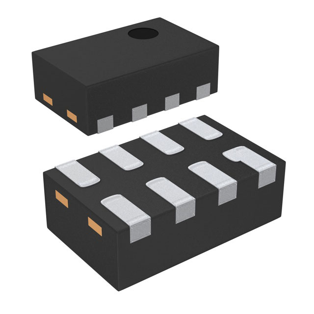
The SLG5NT1462V is a dual-channel power distribution switch IC manufactured by Renesas Electronics. It integrates two independent N-channel load switches with an integrated charge pump, enabling operation from low input voltages. The device supports a supply voltage range of 2.5 V to 5.5 V and delivers high current capability with a maximum continuous output current of 9 A per channel. Key electrical parameters include a maximum on-resistance of 7.3 mΩ, a peak current limit of 12 A, and a maximum power dissipation of 400 mW. It operates within a temperature range of -40°C to +85°C and is housed in an 8-lead DFN package.
Verify the specific suffix variant against the manufacturer's official datasheet to ensure correct pinout and electrical characteristics. Confirm RoHS compliance status through the latest product documentation. Check for obsolescence notices or lifecycle changes directly from Renesas Electronics before finalizing procurement plans.
Select this component when dual isolated power paths are required with high current capacity. The integrated charge pump allows control via standard logic levels even at low supply voltages. Ensure the thermal design accommodates the specified power dissipation limits under maximum load conditions.
This part belongs to Renesas' portfolio of power management ICs, specifically within the load switch category. It complements other power distribution solutions by offering compact integration of dual channels in a small footprint, suitable for space-constrained designs requiring reliable power routing.
Consult Renesas official substitution guides for verified alternatives. Cross-reference pinouts and electrical specifications carefully when considering third-party equivalents to ensure functional compatibility.
The integrated charge pump enables the N-channel MOSFETs to fully turn on even when the input voltage is close to the control signal level, ensuring low on-resistance across the operating range.
Each channel includes built-in overcurrent protection that limits the output current to a maximum of 12 A, protecting both the switch and the connected load from damage during fault conditions.
 SLG5NT1462V
The activity of extra discounts on wholesale prices is in full swing…
Please fill in your contact information and we will send you the latest wholesale price list.