 ChipApex | Global Electronic Components Supplier
SEARCH
Search Product
Search Post
— IC芯片 | 连接器 | 传感器 | 被动器件 —
Search productSearch post
— IC芯片 | 连接器 | 传感器 | 被动器件 —
Consult the customer manager about the wholesale price.
consultation hotline:86-132-6715-2157
email:[email protected]
Contact the product manager for consultation. One-stop consultation is available.
Do you want a lower wholesale price? Please send us your inquiry and we will reply immediately.
The SLG7MD47671V is a high-performance, low-power multi-standard clock generator designed for portable and battery-operated applications. It integrates multiple PLLs to generate precise clock signals from a single input reference. The device supports various output formats including LVCMOS and LVDS, ensuring compatibility with diverse digital systems. Key electrical parameters include an input frequency range of up to 25 MHz and output frequencies configurable via I2C interface. Power consumption is optimized for extended battery life in mobile devices.
Verify the specific suffix 'V' indicates the correct package type and temperature grade. Confirm I2C address settings match your system design. Ensure input reference signal characteristics meet datasheet specifications for optimal performance. Check for any required external components like capacitors or resistors as specified in the application circuit diagram.
Choose this component when multiple clock outputs with different frequencies and standards are required from a single source. Consider its low power profile for battery-sensitive designs. Verify that the available input frequency range matches your system's oscillator. Evaluate the I2C configuration flexibility against your software capabilities.
This part belongs to Renesas' SLG series of programmable clock generators. It is designed to replace discrete clock solutions, reducing board space and complexity. The series is known for high precision and low jitter, making it suitable for high-speed digital interfaces. It complements other Renesas timing products by offering versatile configuration options.
Check for direct pin-to-pin replacements within the same family. Verify functional equivalence regarding output frequencies and power consumption. Ensure the replacement supports the same I2C configuration method. Confirm availability and lead times if switching suppliers.
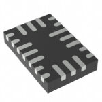 SLG7MD47671V
The activity of extra discounts on wholesale prices is in full swing…
Please fill in your contact information and we will send you the latest wholesale price list.





