 ChipApex | Global Electronic Components Supplier
SEARCH
Search Product
Search Post
— IC芯片 | 连接器 | 传感器 | 被动器件 —
Search productSearch post
— IC芯片 | 连接器 | 传感器 | 被动器件 —
Consult the customer manager about the wholesale price.
consultation hotline:86-132-6715-2157
email:[email protected]
Contact the product manager for consultation. One-stop consultation is available.
Do you want a lower wholesale price? Please send us your inquiry and we will reply immediately.
The SMMBF4393LT1G is an N-channel JFET switching transistor manufactured by onsemi. It features a maximum Drain-Source Voltage (VDS) of 30 Vdc and a Gate-Source Breakdown Voltage (V(BR)GSS) of 30 Vdc. The device has a Zero-Gate-Voltage Drain Current (IDSS) range of 5.0 to 30 mAdc at VDS = 15 Vdc. Static Drain-Source On-Resistance (rDS(on)) is specified at 100 Ohms for ID = 1.0 mAdc. Total Device Dissipation is 225 mW, with a Junction Temperature Range of -55 to +150 °C.
Verify the specific ordering suffix 'S' indicates automotive qualification and unique site requirements. Confirm package type is SOT-23 (TO-236). Ensure compliance with Pb-Free and RoHS standards matches project specifications. Check shipping configuration for tape and reel quantities.
Select this component when low leakage current and high breakdown voltage are required in a small surface-mount package. The S-prefix variant is necessary for automotive supply chain requirements. Compare IDSS ranges against circuit biasing needs to ensure proper turn-off characteristics.
This part belongs to the MMBF439xL family of N-channel JFETs. It shares the same pinout and general electrical limits as MMBF4391LT1G and MMBF4392LT1G but differs in IDSS and rDS(on) parameters. The S-prefix denotes automotive-grade manufacturing.
Direct functional substitutes within the same family include MMBF4391LT1G and MMBF4392LT1G, though IDSS values differ. Non-automotive equivalents are MMBF4393LT1G without the S-prefix.
The device marking code is M6G.
No, the S-prefix indicates automotive qualification and manufacturing site controls; the electrical characteristics remain identical to the commercial version.
The maximum forward gate current (IG(f)) is 50 mAdc.
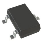 SMMBF4393LT1G
The activity of extra discounts on wholesale prices is in full swing…
Please fill in your contact information and we will send you the latest wholesale price list.






