 ChipApex | Global Electronic Components Supplier
SEARCH
Search Product
Search Post
— IC芯片 | 连接器 | 传感器 | 被动器件 —
Search productSearch post
— IC芯片 | 连接器 | 传感器 | 被动器件 —
Consult the customer manager about the wholesale price.
consultation hotline:86-132-6715-2157
email:[email protected]
Contact the product manager for consultation. One-stop consultation is available.
Do you want a lower wholesale price? Please send us your inquiry and we will reply immediately.
The SN4599DBVRQ1 is an automotive-grade, single-channel, 2:1 (SPDT) analog switch manufactured by Texas Instruments. It operates on a supply voltage range of 2V to 5.5V and supports bidirectional signal paths from GND to VDD. The device features rail-to-rail operation, break-before-make switching, and fail-safe logic on the SEL pin. Key electrical parameters include a maximum on-resistance of 50 Ohms at -40°C to +125°C, a maximum supply current of 35 µA, and a total power dissipation of 300 mW. It is housed in a SOT-23-6 package and qualified under AEC-Q100 for Grade 1 with an operating temperature range of -40°C to +125°C.
Verify the component authenticity through authorized distribution channels or direct manufacturer verification. Confirm that the specific ordering suffix matches the required package type and automotive qualification standards. Ensure the received units align with the documented AEC-Q100 Grade 1 specifications and thermal characteristics before integration into production designs.
Select this component when a single-pole double-throw switch with low on-resistance and wide supply compatibility is required. The fail-safe logic feature makes it suitable for systems where control signals may be active before power-up. Verify that the continuous source/drain current requirements do not exceed the thermal limits defined in the datasheet for the target ambient temperature.
This part belongs to the SN4599-Q1 family of automotive analog switches. It serves as a direct replacement for the NLAS4599-Q1. The device is designed for general-purpose switching applications in harsh automotive environments, offering robust electrostatic discharge protection and reliable performance across the specified industrial temperature range.
The SN4599-Q1 is documented as a direct replacement for the NLAS4599-Q1. Verify pinout compatibility and electrical parameter alignment before substitution. No other substitute part numbers are confirmed in the provided documentation.
The fail-safe logic allows the SEL pin to accept voltages up to 5.5V even if the VDD supply is at 0V. This prevents back-powering the supply rail and removes the requirement for strict power sequencing between the logic control and the supply voltage.
The maximum continuous current (IDC) depends on the junction temperature. At 25°C, it is 150 mA; at 85°C, it is 120 mA; at 125°C, it is 60 mA; and at 130°C, it is 50 mA.
Yes, the SN4599-Q1 supports bidirectional signal paths. Signals can flow equally well from the source pins (S1, S2) to the drain pin (D) or from the drain pin to the source pins, supporting both analog and digital signals within the rail-to-rail range.
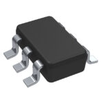 SN4599DBVRQ1
The activity of extra discounts on wholesale prices is in full swing…
Please fill in your contact information and we will send you the latest wholesale price list.





