 ChipApex | Global Electronic Components Supplier
SEARCH
Search Product
Search Post
— IC芯片 | 连接器 | 传感器 | 被动器件 —
Search productSearch post
— IC芯片 | 连接器 | 传感器 | 被动器件 —
Consult the customer manager about the wholesale price.
consultation hotline:86-132-6715-2157
email:[email protected]
Contact the product manager for consultation. One-stop consultation is available.
Do you want a lower wholesale price? Please send us your inquiry and we will reply immediately.
The SN54LS21J is a dual 4-input positive-AND gate manufactured by Texas Instruments. It operates within a supply voltage range of 4.75 V to 5.25 V and supports an operating temperature range of -55 °C to 125 °C. The device utilizes a 14-pin Ceramic Dual In-Line Package (CDIP). Key electrical characteristics include a maximum input clamp current of ±18 mA, a maximum output clamp current of ±20 mA, and a maximum low-level output current of 8 mA.
Verify the specific ordering suffix against the manufacturer's package option addendum to confirm pin count and physical dimensions. Ensure the component meets QML certification requirements if intended for defense applications. Confirm RoHS status and lead finish specifications prior to integration into the bill of materials.
Select this component when designing circuits that require isolated dual four-input AND functionality with high noise immunity. The LS series offers standard TTL compatibility while maintaining lower power consumption compared to earlier standards. Verify that the system voltage remains strictly within the specified 4.75 V to 5.25 V range to ensure reliable operation.
This part belongs to the SN54xx family, which denotes military-grade performance and extended temperature capabilities compared to the commercial SN74xx series. The 'LS' designation indicates Low-power Schottky technology, providing a balance between speed and power dissipation. The 'J' suffix specifically identifies the 14-pin ceramic dual in-line package construction.
Direct replacements include SNJ54LS21W and SNJ54LS21FK, which share identical logical functions but differ in package type. Cross-vendor equivalents from manufacturers such as Motorola or ON Semiconductor may be considered if they meet the same LS-TTL electrical specifications and MIL-STD mechanical constraints.
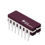 SN54LS21J
The activity of extra discounts on wholesale prices is in full swing…
Please fill in your contact information and we will send you the latest wholesale price list.





