 ChipApex | Global Electronic Components Supplier
SEARCH
Search Product
Search Post
— IC芯片 | 连接器 | 传感器 | 被动器件 —
Search productSearch post
— IC芯片 | 连接器 | 传感器 | 被动器件 —
Consult the customer manager about the wholesale price.
consultation hotline:86-132-6715-2157
email:[email protected]
Contact the product manager for consultation. One-stop consultation is available.
Do you want a lower wholesale price? Please send us your inquiry and we will reply immediately.
The SN65LV1021DBG4 is a serializer component from the Texas Instruments SN65LV1021 series, designed as part of a 10-bit LVDS serdes chipset. It operates with system clock frequencies ranging from 10 MHz to 40 MHz, translating to serial data rates between 120 Mbps and 480 Mbps. The device accepts parallel LVTTL inputs and transmits serialized differential LVDS outputs. It utilizes a 28-pin SSOP package and supports an industrial temperature range of -40°C to +85°C. Power consumption is typically under 350 mW at 40 MHz.
Verify that the specific ordering suffix 'G4' corresponds to lead-free and RoHS-compliant manufacturing standards as defined by Texas Instruments. Confirm the package type matches the required PCB footprint and ensure the operating temperature range aligns with the intended environmental conditions before finalizing procurement.
Select this serializer when paired with the SN65LV1212 deserializer to form a complete 10-bit serdes link. Ensure the design accommodates separate analog and digital power supplies (AVCC and DVCC). Verify that the input clock frequency remains within the specified 10 MHz to 40 MHz range for proper PLL locking and data integrity.
This component belongs to the SN65LV1021 family of LVDS serializers manufactured by Texas Instruments. It serves as the transmitting half of a chipset designed to replace wide parallel buses with serial LVDS links. The device is characterized for industrial temperatures and offers pin-compatible alternatives within the broader LVDS interface portfolio.
The SN65LV1021DB is the non-RoHS equivalent. For deserialization, the SN65LV1212 is the paired component. Check datasheets for any superseding models or updated packaging options if long-term availability is a constraint.
The serializer can transmit specific SYNC patterns consisting of six ones and six zeros. This allows the deserializer to lock to the signal within a deterministic timeframe, rather than waiting for random data transitions.
The TCLK_R/F pin selects the clock edge used to strobe incoming parallel data. Driving it low selects the falling edge, while driving it high selects the rising edge of the TCLK signal.
Driving the PWRDN pin low turns off the internal PLL and places the outputs into a high-impedance state, significantly reducing supply current to the milliampere range.
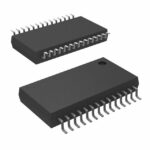 SN65LV1021DBG4
The activity of extra discounts on wholesale prices is in full swing…
Please fill in your contact information and we will send you the latest wholesale price list.





