 ChipApex | Global Electronic Components Supplier
SEARCH
Search Product
Search Post
— IC芯片 | 连接器 | 传感器 | 被动器件 —
Search productSearch post
— IC芯片 | 连接器 | 传感器 | 被动器件 —
Consult the customer manager about the wholesale price.
consultation hotline:86-132-6715-2157
email:[email protected]
Contact the product manager for consultation. One-stop consultation is available.
Do you want a lower wholesale price? Please send us your inquiry and we will reply immediately.
The SN65LV1224BDBG4 is a Texas Instruments LVDS interface integrated circuit functioning as a 1-to-10 deserializer. It converts low-voltage differential signaling (LVDS) serial data into parallel LVTTL or LVCMOS outputs. The device supports data transmission rates up to 660 Mbps and operates on a single 3V to 3.6V power supply. It features an internal phase-locked loop (PLL) for clock recovery, eliminating the need for a separate clock line. The component is housed in a 28-pin SSOP package with surface-mount installation. It includes ESD protection and complies with RoHS standards, operating within a temperature range of -40°C to 85°C.
Verify the specific suffix 'G4' indicates lead-free packaging compliant with RoHS directives. Confirm the 28-SSOP footprint matches the target PCB layout dimensions. Check current manufacturer status as discontinuation notices may affect long-term availability. Ensure voltage levels align with system requirements before integration.
Select this component when a single LVDS input must drive multiple parallel logic lines. Verify that the required data rate does not exceed 660 Mbps. Consider the thermal dissipation capabilities of the SSOP package for the intended environment. Compare against the non-G4 variant if lead-free compliance is not strictly required by regulation.
This part belongs to the SN65LV1224B series of LVDS deserializers from Texas Instruments. It serves as the receiver counterpart to serializers like the SN65LV1023A. The 'G4' suffix specifically denotes a lead-free manufacturing process. It replaces earlier generations such as the DS90LV1224E in modern designs.
The SN65LV1224BDB is a recommended manufacturer substitute. Verify pin compatibility and electrical specifications before swapping. Other family members may offer different packaging options but maintain functional equivalence.
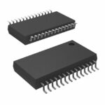 SN65LV1224BDBG4
The activity of extra discounts on wholesale prices is in full swing…
Please fill in your contact information and we will send you the latest wholesale price list.





