 ChipApex | Global Electronic Components Supplier
SEARCH
Search Product
Search Post
— IC芯片 | 连接器 | 传感器 | 被动器件 —
Search productSearch post
— IC芯片 | 连接器 | 传感器 | 被动器件 —
Consult the customer manager about the wholesale price.
consultation hotline:86-132-6715-2157
email:[email protected]
Contact the product manager for consultation. One-stop consultation is available.
Do you want a lower wholesale price? Please send us your inquiry and we will reply immediately.
The SN65LVDS100DGKG4 is a low-voltage differential signaling (LVDS) buffer manufactured by Texas Instruments. It converts LVPECL, CML, or LVDS inputs to LVDS outputs with a data rate of 2 Gbps. The device operates on a single 3.3 V supply and features an 8-pin VSSOP package. Key electrical parameters include a propagation delay of 0.8 ns and a typical power consumption of 12 mA at 3.3 V. It supports input voltage swings from -100 mV to +100 mV and functions within a temperature range of -40°C to +85°C.
Verify the specific suffix 'G4' against the manufacturer's current datasheet to confirm compliance with RoHS directives and lead times. Confirm package availability in VSSOP-8 format. Check for obsolescence notices or lifecycle status updates directly from Texas Instruments documentation before finalizing procurement plans.
Select this component when interfacing between LVPECL/CML sources and LVDS receivers. Ensure the system requires a 2 Gbps data rate capability. Verify that the 8-pin VSSOP footprint matches the PCB layout constraints. Confirm that the 3.3 V operating voltage aligns with the system power rails.
This part belongs to the SN65LVDS100 family of LVDS buffers. It serves as a bridge for signal level translation in high-speed digital interfaces. The DGK package variant indicates a small-outline very thin shrink package. It is designed for applications demanding low skew and precise timing characteristics.
Check for SN65LVDS100D or SN65LVDS100DGKR as potential pin-compatible alternatives. Verify if the base model without the G4 suffix meets environmental requirements. Ensure substitute parts support the same 2 Gbps speed and input/output standards.
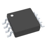 SN65LVDS100DGKG4
The activity of extra discounts on wholesale prices is in full swing…
Please fill in your contact information and we will send you the latest wholesale price list.





