 ChipApex | Global Electronic Components Supplier
SEARCH
Search Product
Search Post
— IC芯片 | 连接器 | 传感器 | 被动器件 —
Search productSearch post
— IC芯片 | 连接器 | 传感器 | 被动器件 —
Consult the customer manager about the wholesale price.
consultation hotline:86-132-6715-2157
email:[email protected]
Contact the product manager for consultation. One-stop consultation is available.
Do you want a lower wholesale price? Please send us your inquiry and we will reply immediately.
The SN65LVDS105DR is a clock fanout buffer manufactured by Texas Instruments, designed to convert a single LVTTL input into four LVDS outputs. It operates within a supply voltage range of 2.97V to 3.63V and supports data rates up to 400Mbps. The device features a typical propagation delay of 2.2ns and offers high ESD protection exceeding 16kV. Packaged in an 8-pin SOIC (DR) format, it functions reliably across an industrial temperature range of -40°C to +85°C.
Verify the specific suffix 'DR' corresponds to the tape-and-reel packaging configuration required for automated assembly processes. Confirm that the component meets RoHS compliance standards applicable to the target market. Ensure the ordering quantity aligns with the manufacturer's standard reel size to avoid partial reel handling issues during procurement.
Select this component when a single LVTTL source must drive multiple LVDS loads with minimal skew. It is suitable for designs requiring 3.3V operation and high-speed clock buffering. Consider the SOIC package constraints regarding thermal dissipation and board space availability compared to other package options in the series.
This part belongs to the SN65LVDS10x family, which includes variants like the SN65LVDS104. While the SN65LVDS104 accepts differential LVDS inputs, the SN65LVDS105 specifically accepts LVTTL inputs. Both share similar output capabilities and are intended for high-speed clock fanout applications requiring low power consumption and noise immunity.
The SN65LVDS105PWG4 serves as a pin-compatible alternative in a TSSOP-16 package. Verify that the pinout differences between the SOIC and TSSOP packages do not require PCB layout modifications before substitution.
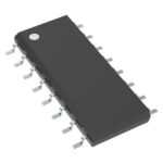 SN65LVDS105DR
The activity of extra discounts on wholesale prices is in full swing…
Please fill in your contact information and we will send you the latest wholesale price list.





