 ChipApex | Global Electronic Components Supplier
SEARCH
Search Product
Search Post
— IC芯片 | 连接器 | 传感器 | 被动器件 —
Search productSearch post
— IC芯片 | 连接器 | 传感器 | 被动器件 —
Consult the customer manager about the wholesale price.
consultation hotline:86-132-6715-2157
email:[email protected]
Contact the product manager for consultation. One-stop consultation is available.
Do you want a lower wholesale price? Please send us your inquiry and we will reply immediately.
The SN65LVDS105PW is a single LVTTL to four LVDS clock fanout buffer manufactured by Texas Instruments. It accepts one low-voltage TTL input and provides four differential LVDS outputs, functioning as a clock distribution component. The device operates within a supply voltage range of 2.4 V to 3.6 V and supports data rates up to 400 Mbps. It features a propagation delay of 2.2 ns and includes ESD protection exceeding 16 kV. The component is housed in a 16-pin TSSOP package and functions reliably across an operating temperature range of -40°C to +85°C.
Verify the specific suffix 'PW' corresponds to the TSSOP-16 package configuration during sourcing. Confirm RoHS compliance status and lead times directly with authorized distributors or Texas Instruments representatives prior to ordering. Ensure the procurement channel is authorized to guarantee component authenticity and traceability.
Select this component when a single LVTTL source must drive multiple LVDS loads with precise timing alignment. Verify that the system power supply remains within the 2.4 V to 3.6 V range. Consider the 2.2 ns propagation delay for timing budget calculations. Ensure the application environment stays within the specified -40°C to +85°C operational temperature limits.
This part belongs to the SN65LVDS10x series, which includes variants like the SN65LVDS104. While the SN65LVDS104 accepts differential LVDS inputs, the SN65LVDS105 specifically accepts LVTTL inputs. Both share similar output configurations and performance characteristics, serving as clock fanout buffers in high-speed digital systems.
The SN65LVDS104 serves as a functional alternative if the input signal is already differential LVDS rather than LVTTL. Other members of the SN65LVDS10x family may offer compatible pinouts but require verification of input logic levels.
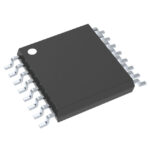 SN65LVDS105PW
The activity of extra discounts on wholesale prices is in full swing…
Please fill in your contact information and we will send you the latest wholesale price list.





