 ChipApex | Global Electronic Components Supplier
SEARCH
Search Product
Search Post
— IC芯片 | 连接器 | 传感器 | 被动器件 —
Search productSearch post
— IC芯片 | 连接器 | 传感器 | 被动器件 —
Consult the customer manager about the wholesale price.
consultation hotline:86-132-6715-2157
email:[email protected]
Contact the product manager for consultation. One-stop consultation is available.
Do you want a lower wholesale price? Please send us your inquiry and we will reply immediately.
The SN65LVDS105PWG4 is a low-voltage differential signaling (LVDS) clock fanout buffer manufactured by Texas Instruments. It accepts one LVTTL input and provides four LVDS outputs, effectively distributing a single clock signal to multiple destinations. The device operates within a supply voltage range of 3.0 V to 3.6 V and functions across an industrial temperature range of -40°C to +85°C. Packaged in a 16-pin Thin Shrink Small Outline Package (TSSOP), it complies with EIA-644 and TIA-644 interface standards. Key electrical characteristics include a maximum high-level input current of 20 µA and a typical propagation delay of 2.7 ns.
Verify the component authenticity by checking the manufacturer's marking code against official documentation. Confirm the package type matches the required PCB footprint specifications. Ensure the operating temperature range aligns with the target application environment. Cross-reference the RoHS compliance status if environmental regulations apply to the final assembly process.
Select this component when a single-ended TTL clock source requires expansion into multiple differential LVDS lines. Consider the 16-pin TSSOP package constraints during layout planning. Evaluate power consumption requirements against the 3.3 V nominal supply voltage. Verify that the input signal levels are compatible with LVTTL logic thresholds before integration.
This part belongs to the SN65LVDS105 family of LVDS clock buffers. It serves as a bridge between legacy LVTTL clock generators and modern LVDS-based receiver circuits. The 'G4' suffix indicates lead-free construction and RoHS compliance. It is distinct from transceivers or serializers, focusing solely on clock fan-out functionality.
Direct replacements may include other SN65LVDS105 variants with different packaging options such as DR or DWR. Verify pin compatibility and electrical parameters before substitution. Generic LVDS buffers with similar I/O configurations require careful validation of timing and voltage levels.
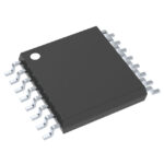 SN65LVDS105PWG4
The activity of extra discounts on wholesale prices is in full swing…
Please fill in your contact information and we will send you the latest wholesale price list.





