 ChipApex | Global Electronic Components Supplier
SEARCH
Search Product
Search Post
— IC芯片 | 连接器 | 传感器 | 被动器件 —
Search productSearch post
— IC芯片 | 连接器 | 传感器 | 被动器件 —
Consult the customer manager about the wholesale price.
consultation hotline:86-132-6715-2157
email:[email protected]
Contact the product manager for consultation. One-stop consultation is available.
Do you want a lower wholesale price? Please send us your inquiry and we will reply immediately.
The SN65LVDS105PWR is a low-voltage differential signaling (LVDS) interface integrated circuit manufactured by Texas Instruments. It functions as a clock fanout buffer featuring one LVTTL input and four LVDS outputs. The device supports data rates up to 400 Mb/s with a typical propagation delay of 2.2 ns. It operates within a supply voltage range of 2.4 V to 3.6 V and draws a maximum operating current of 20 mA. The component is housed in a 16-pin TSSOP package and is rated for an industrial temperature range from -40°C to +85°C.
Verify the suffix 'PW' indicates a tube package while 'PWR' denotes tape-and-reel packaging, as both share the same core electrical specifications. Confirm RoHS compliance status via the manufacturer's official documentation before procurement. Ensure the ordering quantity aligns with the specific reel or tube configuration required for the assembly process.
Select this component when a single LVTTL clock source must drive multiple LVDS loads with minimal skew. It is suitable for designs requiring operation between 2.4 V and 3.6 V. Consider the 16-pin TSSOP footprint for space-constrained layouts. Verify that the target application does not require higher data rates than 400 Mb/s or different input logic levels.
This part belongs to the SN65LVDS10x series, which includes variants like the SN65LVDS104 and SN65LVDS105. The series comprises 4-port LVDS and TTL-to-LVDS repeaters designed for high-speed digital interfaces. The SN65LVDS105 specifically distinguishes itself by accepting LVTTL inputs, whereas other family members may accept differential LVDS inputs.
The SN65LVDS105PWG4 serves as a lead-free variant within the same functional family. Direct substitutes from other manufacturers, such as the STLVDS105, offer similar 4-port LVDS and TTL-to-LVDS repeater functionality but require verification of pinout compatibility and electrical parameter matching.
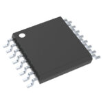 SN65LVDS105PWR
The activity of extra discounts on wholesale prices is in full swing…
Please fill in your contact information and we will send you the latest wholesale price list.





