 ChipApex | Global Electronic Components Supplier
SEARCH
Search Product
Search Post
— IC芯片 | 连接器 | 传感器 | 被动器件 —
Search productSearch post
— IC芯片 | 连接器 | 传感器 | 被动器件 —
Consult the customer manager about the wholesale price.
consultation hotline:86-132-6715-2157
email:[email protected]
Contact the product manager for consultation. One-stop consultation is available.
Do you want a lower wholesale price? Please send us your inquiry and we will reply immediately.
The SN65LVDS108DBTG4 is a clock buffer manufactured by Texas Instruments, designed as an LVDS clock fanout buffer. It features eight outputs and supports a maximum input frequency of 400 MHz. The device operates within a supply voltage range of 3 V to 3.6 V and exhibits a maximum propagation delay of 4.5 ns. It functions reliably across an operating temperature range from -40°C to +85°C. The component is housed in a surface-mount package and is part of the SN65LVDS108 series.
Verify the complete part number including the G4 suffix to ensure compliance with RoHS standards and lead-free manufacturing specifications. Confirm the DBT package type matches the intended PCB footprint. Check humidity sensitivity levels and storage conditions prior to assembly to prevent moisture-related damage during reflow soldering processes.
Select this component when an LVDS-compatible clock buffer with eight outputs is required. Ensure the system design accommodates the specified 3 V to 3.6 V supply voltage range. Verify that the 4.5 ns maximum propagation delay meets the timing constraints of the target application. Consider the SMD/SMT installation style for automated assembly compatibility.
This part belongs to the SN65LVDS108 series of clock buffers from Texas Instruments. It is specifically engineered for low-voltage differential signaling applications. The device serves as a critical interface component for distributing clock signals across multiple loads while maintaining signal integrity in high-speed environments.
Consult official manufacturer documentation for verified substitute part numbers. Cross-reference pinouts and electrical characteristics before implementing any alternative components to ensure functional compatibility.
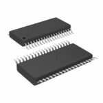 SN65LVDS108DBTG4
The activity of extra discounts on wholesale prices is in full swing…
Please fill in your contact information and we will send you the latest wholesale price list.





