 ChipApex | Global Electronic Components Supplier
SEARCH
Search Product
Search Post
— IC芯片 | 连接器 | 传感器 | 被动器件 —
Search productSearch post
— IC芯片 | 连接器 | 传感器 | 被动器件 —
Consult the customer manager about the wholesale price.
consultation hotline:86-132-6715-2157
email:[email protected]
Contact the product manager for consultation. One-stop consultation is available.
Do you want a lower wholesale price? Please send us your inquiry and we will reply immediately.
The SN65LVDS108DBTRG4 is a low-voltage differential signaling (LVDS) clock fanout buffer manufactured by Texas Instruments. It features one differential input and eight differential outputs, designed to distribute clock signals with high integrity. The device supports maximum input frequencies up to 400 MHz and exhibits a maximum propagation delay of 4.5 ns. It operates within a supply voltage range of 3 V to 3.6 V and functions reliably across an industrial temperature range from -40°C to +85°C. The component is housed in a 38-pin TSSOP package and is supplied in tape-and-reel format for automated surface-mount assembly.
Verify the specific suffix 'G4' confirms lead-free and RoHS compliance status as per manufacturer documentation. Confirm the 'DBT' designation corresponds to the 38-pin TSSOP package variant. Ensure the 'R' suffix indicates tape-and-reel packaging rather than tube packaging when sourcing components for automated production lines.
Select this component when a single differential clock source requires distribution to eight distinct LVDS destinations. Verify that the system power supply remains stable between 3 V and 3.6 V. Ensure the PCB layout accommodates the 38-pin TSSOP footprint and maintains impedance control for differential pairs to preserve signal integrity at frequencies approaching 400 MHz.
This part belongs to the SN65LVDS108 family of LVDS clock buffers. It serves as a derivative of the standard SN65LVDS108, distinguished by its specific packaging and environmental compliance markings. The device is categorized under Clock & Timer ICs within the broader logic and interface integrated circuit portfolio.
The SN65LVDS108DBTR is a non-RoHS compliant alternative within the same package. The SN65LVDS108DBTG4 represents the tube-packaged version of this RoHS-compliant component. Cross-reference datasheets to confirm pin compatibility and electrical specifications before substitution.
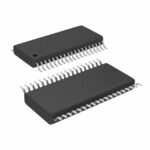 SN65LVDS108DBTRG4
The activity of extra discounts on wholesale prices is in full swing…
Please fill in your contact information and we will send you the latest wholesale price list.





