 ChipApex | Global Electronic Components Supplier
SEARCH
Search Product
Search Post
— IC芯片 | 连接器 | 传感器 | 被动器件 —
Search productSearch post
— IC芯片 | 连接器 | 传感器 | 被动器件 —
Consult the customer manager about the wholesale price.
consultation hotline:86-132-6715-2157
email:[email protected]
Contact the product manager for consultation. One-stop consultation is available.
Do you want a lower wholesale price? Please send us your inquiry and we will reply immediately.
The SN65LVDS109DBT is a dual 4-port LVDS repeater manufactured by Texas Instruments. It operates within a supply voltage range of 3 V to 3.6 V and supports typical data signaling rates up to 400 Mbps. The device features two identical banks, each containing one differential line receiver connected to four differential line drivers. Key electrical parameters include a maximum propagation delay of 4.5 ns, output skew less than 550 ps, bank skew less than 150 ps, and part-to-part skew less than 1.5 ns. It is packaged in a 38-pin Thin Shrink Small-Outline (DBT) package.
Verify the specific ordering suffix 'DBT' corresponds to the 38-pin TSSOP tube packaging configuration. Confirm RoHS compliance status and lead finish details via the manufacturer's current Package Option Addendum. Ensure the procurement channel provides valid traceability documentation for production-grade components.
Select this component when a dual-input, eight-output LVDS splitter is required with tight skew specifications. Compare against the SN65LVDS117 if sixteen outputs per bank are needed. Verify that the 400 Mbps signaling rate meets system requirements and that the DBT package dimensions fit the PCB layout constraints.
This device belongs to the SN65LVDS1xx family of LVDS splitters and repeaters. It shares architectural similarities with the SN65LVDS117 but differs in port count, offering two receivers and eight drivers compared to the SN65LVDS117's sixteen drivers. Both devices utilize the same LVDS signaling technique defined in EIA/TIA-644.
The SN65LVDS117 serves as a higher-density alternative within the same family. No direct single-for-one pin-compatible replacement is documented; design changes may be required for different port counts.
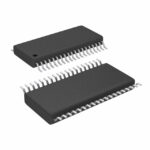 SN65LVDS109DBT
The activity of extra discounts on wholesale prices is in full swing…
Please fill in your contact information and we will send you the latest wholesale price list.





