 ChipApex | Global Electronic Components Supplier
SEARCH
Search Product
Search Post
— IC芯片 | 连接器 | 传感器 | 被动器件 —
Search productSearch post
— IC芯片 | 连接器 | 传感器 | 被动器件 —
Consult the customer manager about the wholesale price.
consultation hotline:86-132-6715-2157
email:[email protected]
Contact the product manager for consultation. One-stop consultation is available.
Do you want a lower wholesale price? Please send us your inquiry and we will reply immediately.
The SN65LVDS109DBTG4 is a dual 4-port LVDS repeater manufactured by Texas Instruments. It integrates two identical banks, each containing one differential line receiver connected to four differential line drivers. The device operates within a supply voltage range of 3 V to 3.6 V and supports typical data signaling rates up to 400 Mbps. Key electrical parameters include a maximum propagation delay of 4.5 ns, an output skew of less than 550 ps, and a bank skew of less than 150 ps. It is housed in a 38-pin Thin Shrink Small-Outline (TSSOP) package.
Verify the specific ordering suffix 'G4' corresponds to lead-free and RoHS-compliant manufacturing standards as defined by Texas Instruments. Confirm that the DBT package designation matches the required 38-pin TSSOP physical dimensions and terminal pitch for your printed circuit board layout. Ensure compatibility with the specified operating temperature range of -40°C to +85°C for your intended environment.
Select this component when a dual-channel LVDS signal splitting solution is required on a single substrate. The integrated design minimizes timing skew compared to using separate devices. Verify that the input signal meets the differential threshold requirements and that the load impedance aligns with the specified 100 Ω termination for optimal signal integrity.
This part belongs to the SN65LVDS10x family of LVDS splitters and repeaters. It shares architectural similarities with the SN65LVDS117 but offers a reduced port count suitable for applications requiring fewer output channels. Both devices utilize the same low-voltage differential signaling protocol to ensure high-speed data transfer with low power consumption.
The SN65LVDS109DBT is the non-green equivalent without the G4 suffix. For higher channel counts, the SN65LVDS117 serves as a functional alternative with eight drivers per bank.
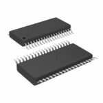 SN65LVDS109DBTG4
The activity of extra discounts on wholesale prices is in full swing…
Please fill in your contact information and we will send you the latest wholesale price list.




