 ChipApex | Global Electronic Components Supplier
SEARCH
Search Product
Search Post
— IC芯片 | 连接器 | 传感器 | 被动器件 —
Search productSearch post
— IC芯片 | 连接器 | 传感器 | 被动器件 —
Consult the customer manager about the wholesale price.
consultation hotline:86-132-6715-2157
email:[email protected]
Contact the product manager for consultation. One-stop consultation is available.
Do you want a lower wholesale price? Please send us your inquiry and we will reply immediately.
The SN65LVDS116DGGG4 is a 1:16 LVDS clock fanout buffer manufactured by Texas Instruments. It operates within an extended temperature range of -40°C to +85°C and utilizes a 64-pin TSSOP package with dimensions of 17 mm in length. The device features differential outputs and accepts differential inputs, complying with EIA-644 and TIA-644 interface standards. It contains 16 drivers with a maximum high-level input current of 0.00002 A. The component is lead-free, RoHS compliant, and classified under ECCN code EAR99.
Verify the complete part number including the G4 suffix to ensure compliance with environmental directives. Confirm the 64-pin TSSOP package variant matches the design footprint. Check for RoHS certification status and lead-free material declarations prior to integration. Ensure the operating temperature range aligns with system requirements.
Select this component when a single LVDS clock source must drive sixteen distinct loads. Verify that the 64-pin TSSOP package fits the available PCB space. Consider the -40°C to +85°C operating range for industrial or automotive environments. Ensure compatibility with EIA-644 standard voltage levels for proper signal interfacing.
This component belongs to the SN65LVDS series of low-voltage differential signaling interface devices from Texas Instruments. It serves as a specialized buffer within the broader family of LVDS transceivers and repeaters designed for high-speed data transmission applications.
The SN65LVDS116DGG is the non-green version of this component. Verify if the RoHS-compliant G4 suffix is required for the specific manufacturing process.
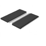 SN65LVDS116DGGG4
The activity of extra discounts on wholesale prices is in full swing…
Please fill in your contact information and we will send you the latest wholesale price list.





