 ChipApex | Global Electronic Components Supplier
SEARCH
Search Product
Search Post
— IC芯片 | 连接器 | 传感器 | 被动器件 —
Search productSearch post
— IC芯片 | 连接器 | 传感器 | 被动器件 —
Consult the customer manager about the wholesale price.
consultation hotline:86-132-6715-2157
email:[email protected]
Contact the product manager for consultation. One-stop consultation is available.
Do you want a lower wholesale price? Please send us your inquiry and we will reply immediately.
The SN65LVDS116DGGR is a Texas Instruments LVDS clock fanout buffer featuring one input and sixteen outputs. It operates within a supply voltage range of 3 V to 3.6 V and supports maximum input frequencies up to 400 MHz. The device exhibits a maximum propagation delay of 4.7 ns. It functions reliably across an operating temperature range from -40 °C to +85 °C. The component is housed in a surface-mount package and supplied in a reel format, suitable for automated assembly processes.
Verify the specific suffix DGGR confirms the tape-and-reel packaging configuration required for your manufacturing line. Confirm that the AEC-Q100 qualification status matches your automotive or industrial reliability standards. Ensure the RoHS compliance documentation aligns with current environmental regulations for your target market. Cross-reference the datasheet revision date to ensure compatibility with your design specifications.
Select this component when a single clock source must drive multiple LVDS loads simultaneously. Verify that the 400 MHz maximum frequency meets your system's timing requirements. Ensure the 3 V to 3.6 V supply voltage range matches your board's power delivery architecture. Consider the 16-output capacity to minimize component count compared to using multiple lower-channel buffers.
This part belongs to the SN65LVDS116 series of LVDS clock buffers manufactured by Texas Instruments. It is categorized under Clock & Timer ICs within the broader interface integrated circuit portfolio. The device is designed to replace older ECL or CMOS clock drivers in high-speed digital systems requiring reduced power consumption and improved noise immunity.
Check for direct pin-compatible alternatives within the same TI LVDS family. Verify if upgraded versions offer enhanced skew performance or additional enable features. Ensure substitute parts maintain the same 1:16 fanout ratio and LVDS output signaling standard.
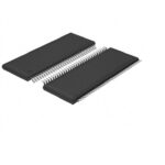 SN65LVDS116DGGR
The activity of extra discounts on wholesale prices is in full swing…
Please fill in your contact information and we will send you the latest wholesale price list.





