 ChipApex | Global Electronic Components Supplier
SEARCH
Search Product
Search Post
— IC芯片 | 连接器 | 传感器 | 被动器件 —
Search productSearch post
— IC芯片 | 连接器 | 传感器 | 被动器件 —
Consult the customer manager about the wholesale price.
consultation hotline:86-132-6715-2157
email:[email protected]
Contact the product manager for consultation. One-stop consultation is available.
Do you want a lower wholesale price? Please send us your inquiry and we will reply immediately.
The SN65LVDS18DRFRG4 is a high-frequency oscillator gain stage and buffer manufactured by Texas Instruments. It operates on a single 2.5-V or 3.3-V supply voltage within an industrial temperature range of -40°C to +85°C. The device features a single-ended input compatible with Low-Voltage PECL levels, providing both differential LVDS outputs (Y and Z) and a configurable Q output. Key electrical parameters include a typical propagation delay of 460 ps, a maximum pulse skew of 80 ps at 3.3 V, and transition times of 250 ps for LVDS signals. The supply current is typically 36 mA when loaded. It is housed in an 8-pin WSON package.
Verify the specific ordering suffix DRFRG4 against the latest Texas Instruments Package Option Addendum to confirm the active production status and tape-and-reel specifications. Ensure that the component's moisture sensitivity level and reflow temperature limits align with your assembly process requirements before finalizing procurement orders.
Select this component when a single-ended low-voltage PECL input must be converted to differential LVDS outputs with adjustable gain. The inclusion of the GC pin allows for precise control over the Q output swing, making it suitable for applications requiring flexible output voltage levels alongside standard differential signaling.
This part belongs to the SN65LVx18 family of oscillator gain stages, which also includes the SN65LVP18, SN65LVDS19, and SN65LVP19 variants. While the SN65LVDS19 offers fully differential inputs, the SN65LVDS18 specifically provides a single-ended input configuration. All devices in this series share similar power supply requirements and packaging options.
The SN65LVP18DRFRG4 serves as a direct functional substitute if LVPECL outputs are required instead of LVDS. For designs needing differential inputs rather than single-ended, the SN65LVDS19DRFRG4 or SN65LVP19DRFRG4 may be appropriate alternatives within the same package footprint.
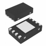 SN65LVDS18DRFRG4
The activity of extra discounts on wholesale prices is in full swing…
Please fill in your contact information and we will send you the latest wholesale price list.





