 ChipApex | Global Electronic Components Supplier
SEARCH
Search Product
Search Post
— IC芯片 | 连接器 | 传感器 | 被动器件 —
Search productSearch post
— IC芯片 | 连接器 | 传感器 | 被动器件 —
Consult the customer manager about the wholesale price.
consultation hotline:86-132-6715-2157
email:[email protected]
Contact the product manager for consultation. One-stop consultation is available.
Do you want a lower wholesale price? Please send us your inquiry and we will reply immediately.
The SN65LVDS19DRFR is a high-frequency oscillator gain stage and buffer manufactured by Texas Instruments. It operates on a single 2.5-V or 3.3-V supply voltage within the -40°C to +85°C temperature range. The device features fully differential LVDS inputs (A, B) and provides two low-voltage PECL or LVDS outputs (Y, Z). It supports clock rates up to 1 GHz with typical intrinsic phase jitter of 0.12 ps at 1 GHz. Propagation delay ranges from 460 ps to 630 ps, while output transition times are typically 250 ps for LVDS and 300 ps for LVPECL. The component is housed in an 8-pin WSON package measuring 2 mm x 2 mm.
Verify the specific ordering suffix against the manufacturer's current Package Option Addendum to confirm active production status and material specifications. Ensure the DRF package designation matches the required 2-mm x 2-mm WSON footprint for PCB layout compatibility. Confirm RoHS compliance and lead finish details prior to final procurement authorization.
Select this component when differential LVDS input is required alongside low-voltage PECL or LVDS outputs. It is appropriate for applications demanding minimal phase jitter and propagation delay under 630 ps. Verify that the system power supply aligns with the 2.5-V or 3.3-V operating range and that the thermal dissipation requirements fit the small-outline no-lead package constraints.
This device belongs to the SN65LVx19 family, which includes variants like SN65LVP19. Unlike the SN65LVDS18, it utilizes fully differential inputs rather than single-ended ones. It serves as a specialized interface solution for converting and amplifying high-frequency clock signals between different logic families in complex electronic architectures.
SN65LVDS19DRFT
The device supports clock rates up to 1 GHz.
It provides an internal voltage reference (VBB), typically 1.35 V below VCC, which can be used to receive single-ended PECL input signals.
The typical intrinsic phase jitter is 0.12 ps when measured at a frequency of 1 GHz.
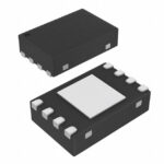 SN65LVDS19DRFR
The activity of extra discounts on wholesale prices is in full swing…
Please fill in your contact information and we will send you the latest wholesale price list.





