 ChipApex | Global Electronic Components Supplier
SEARCH
Search Product
Search Post
— IC芯片 | 连接器 | 传感器 | 被动器件 —
Search productSearch post
— IC芯片 | 连接器 | 传感器 | 被动器件 —
Consult the customer manager about the wholesale price.
consultation hotline:86-132-6715-2157
email:[email protected]
Contact the product manager for consultation. One-stop consultation is available.
Do you want a lower wholesale price? Please send us your inquiry and we will reply immediately.
The SN65LVDS19DRFT is a high-frequency oscillator gain stage and buffer manufactured by Texas Instruments. It operates on a single 2.375-V to 3.6-V supply voltage, supporting both 2.5-V and 3.3-V systems. The device features fully differential LVDS inputs and provides low-voltage PECL or LVDS outputs with clock rates up to 1 GHz. Key electrical parameters include a typical propagation delay of 460 ps, output transition times of 250 ps for LVDS, and an intrinsic phase jitter of 0.12 ps at 1 GHz. It is housed in an 8-pin WSON package.
Verify the specific ordering suffix DRFT corresponds to the required 250-unit small tape-and-reel packaging configuration. Confirm that the component marking ET matches the SN65LVDS19 variant specifications. Ensure compatibility with the specified -40°C to +85°C operating temperature range for the target application environment.
Select this component when a fully differential input interface is required for clock distribution. The SN65LVDS19 differs from the SN65LVDS18 by accepting differential rather than single-ended inputs. Verify that the system design accommodates the 2.5-V or 3.3-V supply requirements and utilizes the appropriate termination networks for the selected output standard.
This part belongs to the SN65LVx18/19 family of oscillator gain stages. It shares the same physical package and general functionality as the SN65LVDS18 but distinguishes itself through its differential input architecture. The family supports both LVDS and LVP (Low-Voltage PECL) output configurations depending on the specific sub-model selected.
SN65LVDS18DRFT: Single-ended input variant with identical package and power characteristics.
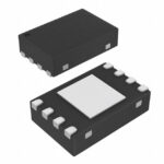 SN65LVDS19DRFT
The activity of extra discounts on wholesale prices is in full swing…
Please fill in your contact information and we will send you the latest wholesale price list.





