 ChipApex | Global Electronic Components Supplier

SEARCH
Search Product
Search Post
— IC芯片 | 连接器 | 传感器 | 被动器件 —
Search productSearch post
— IC芯片 | 连接器 | 传感器 | 被动器件 —
Consult the customer manager about the wholesale price.
consultation hotline:86-132-6715-2157
email:[email protected]
Contact the product manager for consultation. One-stop consultation is available.
Do you want a lower wholesale price? Please send us your inquiry and we will reply immediately.
SN74ACT1073DWR is listed in the Specialty Logic range at ChipApex. The manufacturer field lists Texas Instruments. Its product description is IC 16BIT BUS-TERM ARRAY 20-SOIC. Review the specifications below when checking this part for your BOM.
The SN74ACT1073DWR is a 16-bit bus-termination array with an integrated bus-hold function, manufactured by Texas Instruments. It operates within a supply voltage range of 4.5 V to 5.5 V and supports input voltages up to 5.5 V. The device utilizes a 20-pin SOIC (DW) package for surface-mount installation. It features low power consumption comparable to CMOS technology and includes ESD protection exceeding JESD 22 standards, specifically 2000-V human-body model and 200-V machine model ratings.
Verify the specific ordering suffix to confirm the tape and reel packaging format required for automated assembly processes. Confirm that the active production status aligns with long-term availability requirements for your design lifecycle. Ensure the SOIC package dimensions match your PCB footprint specifications before finalizing procurement orders.
Select this component when designing CMOS systems that require defined voltage levels on floating bus lines. It is suitable for applications needing to reduce signal reflections and maintain data integrity during bus transitions. Consider its TTL compatibility if interfacing with legacy logic families while operating at standard ACT voltage levels.
This part belongs to the SN74ACT series of logic devices, designed for high-speed CMOS applications. It serves as a specialized solution for bus termination and hold functions, distinct from standard flip-flops or buffers. The device integrates both termination and holding capabilities into a single 16-bit channel architecture.
Public confirmed substitute part numbers: SN74ACT1073DW, SN74ACT1073NSR, SN74ACT1073NSR.A.
The bus-hold function uses a CMOS-buffer stage with a high-resistance feedback path between its output and input to keep a bus line tied to the last valid logic state generated by an active driver.
This configuration is designed to minimize high-speed switching noise within the device during operation.
Explore related parts through Logic, Integrated Circuits (ICs), all product categories, ChipApex homepage.
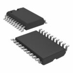 SN74ACT1073DWR

The activity of extra discounts on wholesale prices is in full swing…
Please fill in your contact information and we will send you the latest wholesale price list.





