 ChipApex | Global Electronic Components Supplier

SEARCH
Search Product
Search Post
— IC芯片 | 连接器 | 传感器 | 被动器件 —
Search productSearch post
— IC芯片 | 连接器 | 传感器 | 被动器件 —
Consult the customer manager about the wholesale price.
consultation hotline:86-132-6715-2157
email:[email protected]
Contact the product manager for consultation. One-stop consultation is available.
Do you want a lower wholesale price? Please send us your inquiry and we will reply immediately.
SN74ACT138PWRQ1 is listed in the Signal Switches, Multiplexers, Decoders range at ChipApex. The manufacturer field lists Texas Instruments. Its product description is Automotive 3-Line to 8-Line inve. Review the specifications below when checking this part for your BOM.
The SN74ACT138PWRQ1 is an automotive-grade 3-to-8 decoder/demultiplexer featuring TTL-compatible CMOS inputs. It operates within a supply voltage range of 4.5V to 5.5V and supports continuous output drive currents of ±24mA at 5V, with short-burst capabilities up to ±75mA. The device provides fast propagation delays, typically ranging from 6.6ns to 11ns depending on the input path. It includes three enable inputs (G0, G1, G2) for flexible gating and is qualified under AEC-Q100 standards for Grade 1 temperature operation.
Verify that the specific ordering suffix matches the required package type, as the Q1 series is available in both TSSOP and WQFN configurations. Confirm the presence of wettable flanks if automatic optical inspection compatibility is a design requirement. Ensure the selected variant meets the specific thermal and electrical constraints defined in the datasheet's absolute maximum ratings table.
Select this component when designing systems requiring robust interface between 5V logic and lower voltage microcontrollers due to its TTL-compatible input thresholds. Consider the device's high output drive strength for applications involving long traces or heavy capacitive loads. Verify that the chosen package style aligns with the board layout constraints and manufacturing inspection capabilities regarding lead visibility.
This part belongs to the SN74ACT138-Q1 family of automotive decoders. It shares functional logic with standard industrial counterparts but incorporates enhanced reliability features and qualification testing mandated for automotive environments. The 'Q1' designation indicates compliance with AEC-Q100 standards, distinguishing it from non-automotive variants like the SN74ACT138PWR.
SN74ACT138WBQBRQ1
Unused TTL-compatible CMOS inputs must not be left floating. They should be terminated directly to VCC or ground, or connected via a pull-up/pull-down resistor to ensure valid logic states during operation.
These are output strobe inputs used to enable or disable the decoder outputs. G2 is active-high, while G1 and G0 are active-low. If any strobe condition is unmet, all outputs are forced to the high state regardless of address inputs.
Explore related parts through Logic, Integrated Circuits (ICs), all product categories, ChipApex homepage.
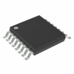 SN74ACT138PWRQ1

The activity of extra discounts on wholesale prices is in full swing…
Please fill in your contact information and we will send you the latest wholesale price list.






