 ChipApex | Global Electronic Components Supplier

SEARCH
Search Product
Search Post
— IC芯片 | 连接器 | 传感器 | 被动器件 —
Search productSearch post
— IC芯片 | 连接器 | 传感器 | 被动器件 —
Consult the customer manager about the wholesale price.
consultation hotline:86-132-6715-2157
email:[email protected]
Contact the product manager for consultation. One-stop consultation is available.
Do you want a lower wholesale price? Please send us your inquiry and we will reply immediately.
SN74ACT139PWR is listed in the Signal Switches, Multiplexers, Decoders range at ChipApex. The manufacturer field lists Texas Instruments. Its product description is DUAL 2-LINE TO 4-LINE DECODER AN. Review the specifications below when checking this part for your BOM.
The SN74ACT139PWR is a dual 2-to-4 decoder and demultiplexer from the Texas Instruments ACT logic family. It operates within a supply voltage range of 4.5V to 5.5V and features TTL-compatible inputs. The device provides balanced CMOS push-pull outputs capable of continuous ±24mA drive, with short burst support up to ±75mA. Propagation delays are specified at a maximum of 10.2ns for address transitions and 10.4ns for strobe transitions. It is housed in a 16-pin TSSOP package and supports an operating temperature range from -40°C to +125°C.
Verify the specific ordering suffix against the manufacturer's official documentation to confirm packaging details and material specifications. Ensure that the selected variant matches the required thermal performance and moisture sensitivity level for the intended manufacturing process. Cross-reference the part number with the latest datasheet revision history to validate current production status and availability constraints.
Select this component when system design requires high-speed decoding with TTL input compatibility. The ACT series offers faster switching speeds compared to standard HC logic while maintaining CMOS power efficiency. Consider the thermal characteristics and output drive capabilities when designing for heavy capacitive loads or high-frequency operation environments.
This device belongs to the SN74ACT series, representing advanced CMOS technology optimized for speed and low power consumption. It serves as a logical evolution in Texas Instruments' logic portfolio, providing enhanced performance metrics over previous generations while maintaining pinout compatibility with legacy designs.
SN74ACT139PW
The demultiplexing function utilizes the address select inputs to choose the desired output line, while the strobe input acts as the data input. When the strobe is active (LOW), the data appears non-inverted at the selected output.
Unused TTL-compatible CMOS inputs must not be left floating. They should be terminated to VCC or GND, potentially using a pull-up or pull-down resistor, to prevent oscillations and excessive power consumption.
Explore related parts through Logic, Integrated Circuits (ICs), all product categories, ChipApex homepage.
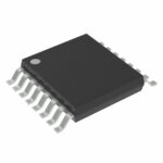 SN74ACT139PWR

The activity of extra discounts on wholesale prices is in full swing…
Please fill in your contact information and we will send you the latest wholesale price list.





