 ChipApex | Global Electronic Components Supplier
SN74ACT3632-20PCB
Search Product
Search Post
— IC芯片 | 连接器 | 传感器 | 被动器件 —
Search productSearch post
— IC芯片 | 连接器 | 传感器 | 被动器件 —
Consult the customer manager about the wholesale price.
consultation hotline:86-132-6715-2157
email:[email protected]
Contact the product manager for consultation. One-stop consultation is available.
Do you want a lower wholesale price? Please send us your inquiry and we will reply immediately.
The SN74ACT3632-20PCB is a high-speed, low-power CMOS clocked bidirectional FIFO memory featuring two independent 512 × 36 dual-port SRAMs. It supports clock frequencies up to 67 MHz with read access times as fast as 11 ns. The device includes programmable almost-full and almost-empty flags synchronized to respective port clocks. Each FIFO has a 36-bit mailbox-bypass register for direct data transfer. It operates from 0°C to 70°C in a 120-pin Thin Quad Flat (PCB) package.
Verify the specific ordering suffix PCB confirms the 120-pin Thin Quad Flat package type. Confirm the -20 speed grade matches the required 11 ns access time specifications. Ensure the operating temperature range of 0°C to 70°C aligns with the target environment requirements before procurement.
Select this component when bidirectional data flow requires independent clock domains for each port. The device is suitable for applications needing programmable flag offsets for precise buffer management. Consider the 120-pin PCB package constraints for board layout. Verify compatibility with existing logic families if voltage levels differ from standard ACT specifications.
This part belongs to the SN74ACT3632 family of clocked bidirectional FIFO memories. It is pin-to-pin compatible with the SN74ACT3622 and SN74ACT3642 variants. The device utilizes low-power 0.8-micron Advanced CMOS technology. It is characterized for commercial operation within a specified temperature range.
The SN74ACT3622 and SN74ACT3642 are confirmed pin-to-pin compatible substitutes within the same product family.
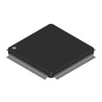 SN74ACT3632-20PCB
The activity of extra discounts on wholesale prices is in full swing…
Please fill in your contact information and we will send you the latest wholesale price list.





