 ChipApex | Global Electronic Components Supplier
SEARCH
Search Product
Search Post
— IC芯片 | 连接器 | 传感器 | 被动器件 —
Search productSearch post
— IC芯片 | 连接器 | 传感器 | 被动器件 —
Consult the customer manager about the wholesale price.
consultation hotline:86-132-6715-2157
email:[email protected]
Contact the product manager for consultation. One-stop consultation is available.
Do you want a lower wholesale price? Please send us your inquiry and we will reply immediately.
The SN74ACT3651-15PCB is a high-speed, low-power CMOS clocked FIFO memory featuring a 2048 x 36 dual-port SRAM architecture. It supports independent asynchronous or coincident clocks for Port A and Port B, enabling data buffering between ports with read access times as fast as 11 ns. The device operates within a voltage range of 4.5 V to 5.5 V and is characterized for temperatures from 0°C to 70°C. It includes retransmit capability, mailbox registers, and programmable flags.
Verify the package type matches the PCB designation (120-pin Thin Quad Flat). Confirm the suffix -15 indicates the specified 11 ns access time variant. Ensure the operating temperature range meets the application requirements of 0°C to 70°C. Check for RoHS compliance status if required by the manufacturing process.
Select this component when a dual-port FIFO with independent clock domains is required for buffering data between asynchronous or coincident systems. Consider the 36-bit data width and 2048-word depth against system bandwidth needs. Evaluate the need for retransmit functionality and mailbox registers for control signaling before choosing alternative single-port or narrower-width FIFOs.
This part belongs to the SN74ACT3651 family of clocked FIFO memories manufactured by Texas Instruments. It is pin-to-pin compatible with the SN74ACT3631 and SN74ACT3641 models, facilitating design upgrades or replacements within existing hardware architectures without requiring board layout changes.
The SN74ACT3631 and SN74ACT3641 are confirmed pin-compatible substitutes within the same product family.
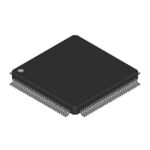 SN74ACT3651-15PCB
The activity of extra discounts on wholesale prices is in full swing…
Please fill in your contact information and we will send you the latest wholesale price list.






