 ChipApex | Global Electronic Components Supplier
SEARCH
Search Product
Search Post
— IC芯片 | 连接器 | 传感器 | 被动器件 —
Search productSearch post
— IC芯片 | 连接器 | 传感器 | 被动器件 —
Consult the customer manager about the wholesale price.
consultation hotline:86-132-6715-2157
email:[email protected]
Contact the product manager for consultation. One-stop consultation is available.
Do you want a lower wholesale price? Please send us your inquiry and we will reply immediately.
The SN74ACT3651-20PCB is a high-speed, low-power CMOS clocked FIFO memory with a 2048 x 36 configuration. It supports clock frequencies up to 67 MHz and features fast access times of 11 ns. The device buffers data from Port A to Port B using independent synchronous interfaces. It includes retransmit capability, two 36-bit mailbox registers for control communication, and programmable almost-full and almost-empty flags. The component operates within a temperature range of 0°C to 70°C.
Verify the specific ordering suffix PCB confirms the 120-pin Thin Quad Flat package variant. Confirm the revision level matches SCAS439D – Revised February 1999 specifications. Ensure the supply source provides production data consistent with Texas Instruments standard warranty terms. Check for RoHS compliance details if required by the target assembly process.
Select this component when a 36-bit wide data path is required for high-speed buffering. It is suitable for systems needing independent port clocks that may operate asynchronously. Consider its pin-to-pin compatibility with SN74ACT3631 and SN74ACT3641 if upgrading existing designs. Evaluate the need for retransmit functionality and mailbox registers for complex control logic integration.
This part belongs to the SN74ACT series of advanced CMOS logic devices manufactured by Texas Instruments. It is functionally related to the SN74ACT3631 and SN74ACT3641 models, offering pin-compatible alternatives within the same family. The device utilizes low-power 0.8-micron technology to achieve high performance while maintaining power efficiency standards typical of the ACT logic family.
The SN74ACT3651 is pin-to-pin compatible with the SN74ACT3631 and SN74ACT3641. Verify that the substitute part number matches the specific package type and electrical characteristics required for the application.
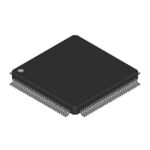 SN74ACT3651-20PCB
The activity of extra discounts on wholesale prices is in full swing…
Please fill in your contact information and we will send you the latest wholesale price list.





