 ChipApex | Global Electronic Components Supplier
SEARCH
Search Product
Search Post
— IC芯片 | 连接器 | 传感器 | 被动器件 —
Search productSearch post
— IC芯片 | 连接器 | 传感器 | 被动器件 —
Consult the customer manager about the wholesale price.
consultation hotline:86-132-6715-2157
email:[email protected]
Contact the product manager for consultation. One-stop consultation is available.
Do you want a lower wholesale price? Please send us your inquiry and we will reply immediately.
The SN74ACT3651 is a high-speed, low-power CMOS clocked FIFO memory featuring a 2048 × 36 dual-port SRAM array. It supports clock frequencies up to 67 MHz and provides fast access times of 11 ns. The device includes retransmit capability, allowing previously read data to be accessed again. Communication between ports utilizes two 36-bit mailbox registers with dedicated flags. Status flags including input-ready, output-ready, almost-full, and almost-empty are synchronized to their respective port clocks.
Verify the specific package variant required, as the SN74ACT3651 family includes both 120-pin Thin Quad Flat (PCB) and 132-pin Plastic Quad Flat (PQ) options. Confirm that the ordering suffix matches the desired physical footprint and pin configuration. Ensure compatibility with existing board layouts before procurement, as these packages are not interchangeable without design modification.
Select this component when designing systems requiring high-speed data buffering between asynchronous domains. The ACT series offers low power consumption suitable for battery-operated or heat-sensitive environments. Consider the 11 ns access time and 67 MHz clock support for high-throughput applications. Verify that the 36-bit data width aligns with system bus requirements or allows for efficient parallel expansion.
This part belongs to the SN74ACT logic family, utilizing low-power 0.8-μm Advanced CMOS technology. It is pin-to-pin compatible with the SN74ACT3631 and SN74ACT3641 models, facilitating direct upgrades or replacements within existing designs. The device is characterized for operation from 0°C to 70°C, covering standard commercial temperature ranges.
The SN74ACT3651 is pin-to-pin compatible with the SN74ACT3631 and SN74ACT3641.
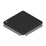 SN74ACT3651-30PCB
The activity of extra discounts on wholesale prices is in full swing…
Please fill in your contact information and we will send you the latest wholesale price list.





